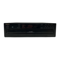
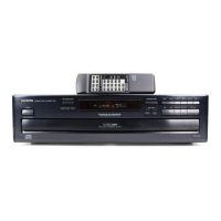
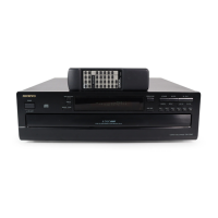
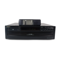
DX-C390
IC BLOCK DIAGRAM/ TERMINAL DESCRIPTION
Q501 : LC78683E MP3 DECODER FOR CD
Continued from preceding page.
Pin No. Pin Name I/O Block Function
51 DV
DD
4 Digital I/O system power supply
52 V
SS
Power supply
Ground
53 MADRS7 O DRAM address output 7
54 MADRS6 O DRAM address output 6
55 MADRS5 O DRAM address output 5
56 MADRS4 O DRAM address output 4
57 MADRS3 O DRAM address output 3
58 MADRS2 O DRAM address output 2
59 MADRS1 O DRAM address output 1
60 MADRS0 O
Memory interface
DRAM address output 0
61 DV
DD
5 Internal logic system power supply
62 V
SS
Power supply
GND
63 STREQ I/O
MP3 data request flag output (active high)
/DRAM data request flag input (CD-ROM mode, active high)
64 STCK I/O
MP3 data transfer clock input
/DRAM data transfer clock output
65 STDAT I/O
MP3 stream I/O
MP3 serial data input
/DRAM serial data output
66 FSYNC O MP3-dec
MP3 frame sync signal (active high)
/Data continuity point detection complete flag (CD-DA mode, active high)
67 CRCF O CD monitor
CRC check result output (CD-ROM data/CD-DA subcode data)
/DRAM data output enable signal output (active high)
68 DV
DD
6 Digital I/O system power supply
69 V
SS
Power supply
GND
70 WOK I
DRAM write enable input (CD-DA mode, active high)
/DRAM data request flag input
71 CNTOK O
Data continuity point detection complete flag (CD-DA mode, active high)
/SYNC error monitor flag (MP3 mode, active high)/DRAM serial data output
72 OVF O
CD-DA shockproof
and MP3 I/O
DRAM write interrupt flag (CD-DA mode, active high)
/Emphasis output flag (CD-DA and MP3 modes, active high)
/DRAM data transfer clock output
73 CMDOUT O Serial command data output (n-channel open-drain output)
74 CMDIN I Serial command data input
75 CL I Serial command clock input
76 CE I Command enable input (active high)
77 INTB O
Interrupt signal output (active low)
/DRAM write interrupt flag (CD-DA mode, active high)
78 RESB I
Microcontroller
interface
System reset (active low)
79 DATAIN I Serial CD data input
80 DATACK I
CD IF
CD bit clock input
Notes: 1. Notes on unused pins.
Unused input pins must be connected to the ground level (0 V).
Unused output pins must be left open. Do not connect anything to these pins.
Unused I/O pins may either be connected to the ground level (0 V) or set to output mode and left open.
2. The corresponding power supply levels must be provided to all of the DV
DD
1, DV
DD
3, DV
DD
4, DV
DD
6, and AV
DD
pins. The
corresponding power supply level must also be provided to DV
DD
2 and DV
DD
5. (See the Allowable Operating Ranges specifications for
the supply levels.)
3. The TEST1 and TEST2 input pins must be connected to ground (0 V).
4. The I/O pins (MDAT0:15, STREQ, STCK, and STDAT) go to input mode after a reset.
5. After first applying the power supply levels, the RESB pin must be held low for at least 1 µs.
6. A 16.9344 MHz clock signal must be supplied to the CKIN pin by the CD DSP.
The LC78684E does not support the implementation of an oscillator circuit using an oscillator element.
 Loading...