E-935-1-E
10
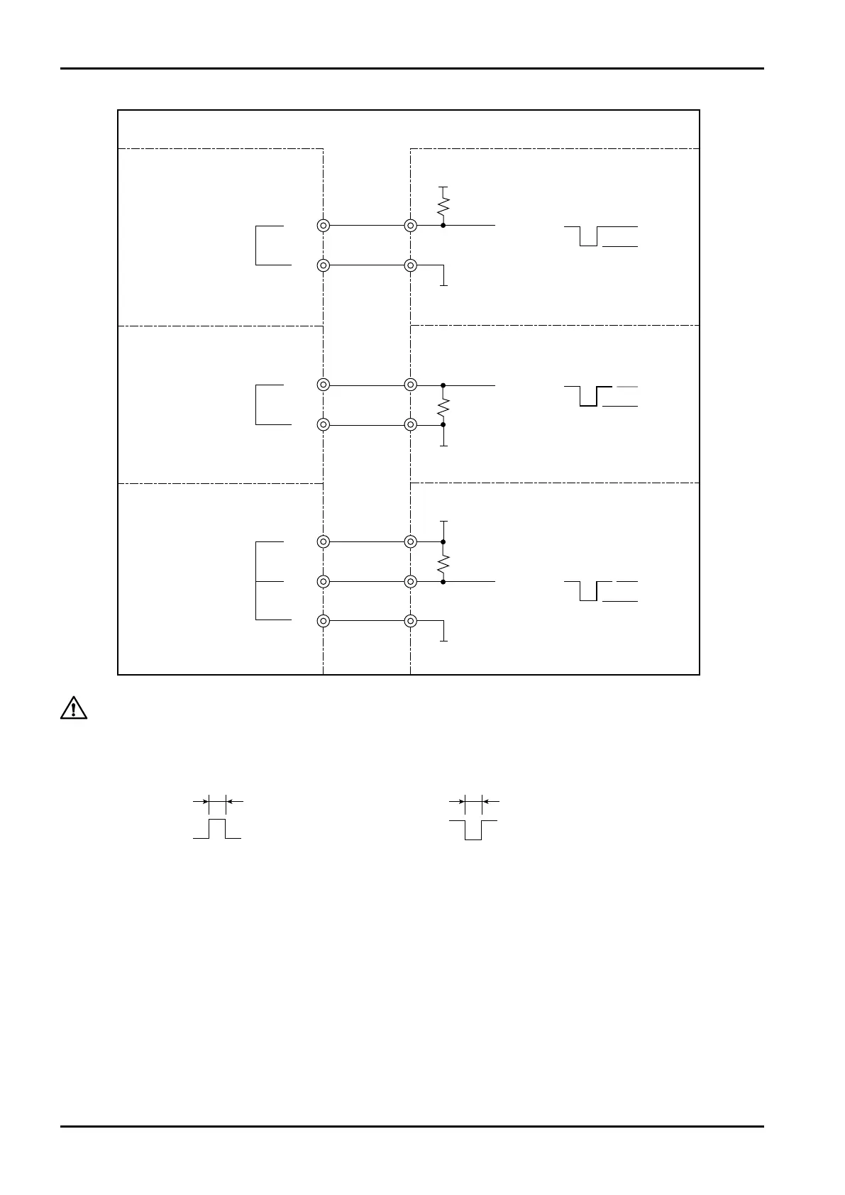
SIG
0V
SIG
0V
SUP
SIG
0V
Vcc(13.5V)
GND(0V)
13.4V
0.1V
[O.C]
GND(0V)
10kΩ(RECOMMENDATION)
10kΩ(RECOMMENDATION)
(R=10kΩ)
(R=10kΩ)
(R=10kΩ)
5.1V
0.1V
[VOLT]
[PA11]
Vcc(32V)
GND(0V)
10kΩmin.
31.9V
1.0V
30mA
0.25or1or50ms0.25or1or50ms
PC2201
RECEIVING
INSTRUMENT
(SIG.WAVEFORM)
SIG
0V
SIG
0V
SUP
SIG
0V
Vcc(13.5V)
GND(0V)
13.4V
0.1V
[O.C]
GND(0V)
10kΩ(RECOMMENDATION)
10kΩ(RECOMMENDATION)
(R=10kΩ)
(R=10kΩ)
(R=10kΩ)
5.1V
0.1V
[VOLT]
[PA11]
Vcc(32V)
GND(0V)
10kΩmin.
31.9V
1.0V
30mA
0.25or1or50ms0.25or1or50ms
PC2201
RECEIVING
INSTRUMENT
(SIG.WAVEFORM)
・
Voltage levels of signal waveform include an error of
±
0.5V.
・
Signal waveforms shown here indicate the position of fixed width when a fixed pulse width
is
chosen.
CAUTION:
・
In case of “PG20”, “O.C.” and “PA11”, because of a 200
Ω
protective resistor in series with
the “SIG” output, voltage level L
0
of signal waveform varies with the resistance value of
the shunt resistor coupled to the power in the receiving instrument.
Voltage level L
0
[
V
]≒
voltage Vcc
[
V
]÷
shunt resistance value
[Ω]×
200
[Ω]
+
PC2201 output transistor “ON” voltage (0
to
0.5)
[
V
]