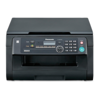
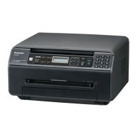
KX-MB262CX/KX-MB772CXKX-MB262CX/KX-MB772CX
When CHG REM is “L”, 5.425kHz PWM (Pulse Width Modulation) is input from IC300 to DEV CLK through Q504, developingWhen CHG REM is “L”, 5.425kHz PWM (Pulse Width Modulation) is input from IC300 to DEV CLK through Q504, developing
voltage corresponding to the DUTY of PWM signal voltage corresponding to the DUTY of PWM signal
is output from DEV OUTPUTis output from DEV OUTPUT
. Also DUTY is adjusted by . Also DUTY is adjusted by
the utilization of thethe utilization of the
developing unit and developing unit and
environmental temperature.environmental temperature.
330 Vp-p 34 kHz wave of developing AC voltage is output from DEV OUTPUT. This voltage is overlapped with developing DC330 Vp-p 34 kHz wave of developing AC voltage is output from DEV OUTPUT. This voltage is overlapped with developing DC
voltage and output as AC voltage that includes the voltage and output as AC voltage that includes the
development DC voltage.development DC voltage.
When CHG REM is “L” and TRA CLK is “open”, Charge BIAS (200When CHG REM is “L” and TRA CLK is “open”, Charge BIAS (200
Transfer (+) BIAS (785V) is output from TRA OUTPUT. When 5.086kHz PWM (Pulse Width Modulation) signal is input to TRATransfer (+) BIAS (785V) is output from TRA OUTPUT. When 5.086kHz PWM (Pulse Width Modulation) signal is input to TRA
CLK through transistor Q501, Transfer (-) CURRENT BIAS corresponding to CLK through transistor Q501, Transfer (-) CURRENT BIAS corresponding to
PWM signal is output PWM signal is output
from TRA OUTPUTfrom TRA OUTPUT
 Loading...