EasyManua.ls Logo

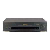
Panasonic NV-SV120EG - User Manual

Panasonic NV-SV120EG
138 pages
Print Icon
To Next Page IconTo Next Page
Loading...
ORDER NO. MABR0303007C2
Video Cassette Recorder
NV-SV120EG
Z-MECHANISM
SPECIFICATIONS
2003 Matsushita Electric Industrial Co., Ltd. All rights reserved.
Unauthorized copying and distribution is a violation of law.
1. INTRODUCTION
1.1. INTRODUCTION
This service manual contains technical information which will allow service personnel to
understand and service this model.
1
Question and Answer IconNeed help?

Do you have a question about the Panasonic NV-SV120EG and is the answer not in the manual?

Summary

1. INTRODUCTION

1.2. ABOUT LEAD FREE SOLDER (PbF)

Information regarding the distinction and handling of lead-free solder (PbF) used in PCBs.

2. GENERAL DESCRIPTIONS

2.1. SERVICE CAUTION

Important precautions and warnings for service personnel regarding general operations and component handling.

2.1.2. CYLINDER UNIT REPLACEMENT

Detailed procedure for the replacement of the cylinder unit, including disassembly and reassembly steps.

2.1.3. CHECKING OF MAIN C.B.A.

Steps for checking the main circuit board assembly (C.B.A.) during servicing operations.

2.1.4. FLAT CARD CABLE INSTALLATION

Guidelines for the correct installation of flat card cables onto their connectors.

2.2. REMOVAL OF CASSETTE TAPE

Procedures for safely removing a cassette tape from the VCR unit.

2.3. INTRODUCTION OF VIDEO HEAD CLEANING CASSETTE; (POLISHING TYPE )

Introduction to Panasonic video head cleaning cassettes for service purposes.

2.4. SELF-DIAGNOSIS RESULT DISPLAY

Explanation of the VTR's self-diagnosis function and how to display error codes.

3. ADJUSTMENT PROCEDURES

3.1. DISASSEMBLY METHOD

Provides a flow chart and details for disassembling the product for servicing.

3.1.2. DETAIL OF DISASSEMBLY METHOD

Step-by-step instructions for detailed disassembly of unit components.

3.2. MECHANICAL ADJUSTMENT PROCEDURES

Procedures for performing mechanical adjustments on the device.

3.3. ELECTRICAL ADJUSTMENT PROCEDURES

Procedures for performing electrical adjustments, including required test equipment.

3.3.3. ADJUSTMENTS

General adjustments required for the device, including tape speed and channel settings.

3.3.5. S-VHS VIDEO FREQUENCY RESPONSE ADJUSTMENT

Procedure for adjusting the S-VHS video frequency response.

3.3.6. VHS VIDEO FREQUENCY RESPONSE ADJUSTMENT

Procedure for adjusting the VHS video frequency response.

3.3.7. LOCATION OF TEST POINTS & CONTROLS

Identification and location of essential test points and controls for adjustments.

4. ABBREVIATIONS

5. INPUT;OUTPUT CHART

5.1. INPUT;OUTPUT CHART FOR IC6001

Detailed chart of input and output signals for IC6001.

5.2. TRUTH TABLE

A table outlining the truth values or logical states for specific functions.

6. WAVEFORM TABLE & VOLTAGE CHART

6.1. WAVEFORM TABLE

A table listing expected waveforms at various test points.

6.2. VOLTAGE CHART

A chart detailing voltage measurements at different points in the circuit.

7. BLOCK DIAGRAMS

7.1. SYSTEM CONTROL & SERVO BLOCK DIAGRAM

A block diagram illustrating the system control and servo functions.

7.2. LUMINANCE & CHROMINANCE BLOCK DIAGRAM

A block diagram showing the luminance and chrominance signal processing path.

7.3. S-VHS BLOCK DIAGRAM

A block diagram specific to the S-VHS signal processing.

7.4. AUDIO BLOCK DIAGRAM

A block diagram illustrating the audio signal processing paths.

8. SCHEMATIC DIAGRAMS

8.1. POWER TRANSFORMER SECTION IN MAIN SCHEMATIC DIAGRAM

Schematic diagram of the power transformer section within the main circuit.

8.2. POWER SUPPLY; RF SECTION IN MAIN SCHEMATIC DIAGRAM

Schematic diagram of the power supply and RF sections.

8.3. TIMER SECTION IN MAIN SCHEMATIC DIAGRAM

Schematic diagram of the timer circuit within the main unit.

8.4. SYSTEM CONTROL & SERVO SECTION IN MAIN SCHEMATIC DIAGRAM

Schematic diagram of the system control and servo circuits.

8.5. LUMINANCE & CHROMINANCE; AUDIO SECTION IN MAIN SCHEMATIC DIAGRAM

Schematic diagram for luminance, chrominance, and audio signal processing.

8.6. Hi-Fi AUDIO SECTION IN MAIN SCHEMATIC DIAGRAM

Schematic diagram detailing the Hi-Fi audio circuitry.

8.7. INPUT; OUTPUT SECTION IN MAIN SCHEMATIC DIAGRAM

Schematic diagram illustrating the input and output signal paths.

8.8. DECODER SECTION IN MAIN SCHEMATIC DIAGRAM

Schematic diagram of the decoder section.

8.9. TV DEMODULATOR PACK SCHEMATIC DIAGRAM

Schematic diagram for the TV demodulator pack.

8.10. S-VHS PACK SCHEMATIC DIAGRAM

Schematic diagram for the S-VHS pack.

8.11. FRONT SCHEMATIC DIAGRAM

Schematic diagram of the front panel circuitry.

8.12. CYLINDER STATOR UNIT SCHEMATIC DIAGRAM

Schematic diagram for the cylinder stator unit.

8.13. CAPSTAN UNIT SCHEMATIC DIAGRAM

Schematic diagram for the capstan unit.

9. CIRCUIT BOARD ASSEMBLIES

9.1. TV DEMODULATOR PACK C.B.A.

Circuit board assembly details for the TV demodulator pack.

9.2. CYLINDER STATOR UNIT

Circuit board assembly details for the cylinder stator unit.

9.3. FRONT C.B.A.

Circuit board assembly details for the front panel.

9.4. MAIN C.B.A.

Circuit board assembly details for the main unit.

9.5. S-VHS PACK C.B.A.

Circuit board assembly details for the S-VHS pack.

10. EXPLODED VIEWS

10.1. CHASSIS PARTS SECTION

Exploded view illustrating the chassis parts of the unit.

10.2. CASING PARTS SECTION

Exploded view illustrating the casing parts of the unit.

10.3. PACKING PARTS SECTION

Exploded view illustrating the packing parts of the unit.

11. REPLACEMENT PARTS LIST

11.1. CHASSIS PARTS SECTION PARTS LIST

List of replaceable chassis parts with their corresponding details.

11.2. CASING PARTS SECTION PARTS LIST

List of replaceable casing parts with their corresponding details.

11.3. PACKING PARTS SECTION PARTS LIST

List of replaceable packing parts with their corresponding details.

11.4. ELECTRICAL PARTS LIST

List of replaceable electrical components with their part numbers and descriptions.

How to replace the Fuse

Panasonic NV-SV120EG Specifications

General IconGeneral
TypeVCR
Video SystemPAL
TunerYes
Hi-Fi AudioYes
ShowviewYes
Remote ControlYes
On-Screen DisplayYes
TimerYes
Recording SpeedSP, LP
Playback SpeedSP, LP
ConnectionsRF
Video Head4-head
Recording SystemRotary 4-head helical scan

Related product manuals