Pin
No.
Terminal
Name
I/O Function
41 FEN I Focus error signal amp inverting input
42 TEN I Tracking error signal amp inverting input
43 TEOUT O Tracking error signal amp output
44 VREF O VREF output
45 DUTYADJ I Laser intermittent drive clock duty adj.
resistor terminal
46 CKMON - Not used, open
47 PD I APC amp input
48 LD O Laser power drive signal output
49 VDDDRV I Power supply terminal
50 CLD I APC loop filter connected terminal
51 VDDLD I Power supply terminal
52 E I Tracking signal input 1
53 F I Tracking signal input 2
54 B I Focus signal input 2/RF addition amp
input 2
55 C I RF addition amp input 3
56 A I Focus signal input 1/RF addition amp
input 1
57 DCDET I HPF capacitor connected terminal
58 RFVDD I Power supply terminal
59 RFN - Not used, open
60 RFOUT - Not used, open
61 RFIN I AGC input
62 CAGC I AGC loop filter capacitor connected terminal
63 ARFOUT O AGC output
64 AVSS2 - GND
65 ARFIN I RF signal input
66 DSLF O Loop filter for DSL
67 IREF I Reference current input
68 PLLF O Loop filter for PLL
69 PLLFO O Loop filter for PLL
70 AVDD2 I Power supply terminal
71 LOOUTL - Not used, open
72 AVSS1 - GND
73 AVREF - Not used, open
74 LOOUTR - Not used, open
75 AVDD1 I Power supply terminal
76 HPCNT I Headphone control signal input
77 HPVDDL I Power supply terminal
78 HPOUTL O L ch audio output for headphone
79 HPVSSL - GND
80 HPVDDR I Power supply terminal
81 HPOUTR O R ch audio output for headphone
82 HPVSSR - GND
83 NTEST I Test mode input
84 DVSS2 - GND
85 X1 I Crystal oscillator connected terminal
(F=16.9 MHz)
86 X2 O
87 IOVDD2 I Power supply terminal
88 DVDD2 I Power supply terminal
89 VM4SEL/
OFF
- Not used, open
90 PMSEL1/
FBAL
I Connected to power supply via resistor
91 PMSEL2/
TBAL
- Not used, open
92 LASER
SEL/BDO
- Not used, open
93 CLVS/
RFDET
- Not used, open
94 IPFLAG2/
VDET
- Not used, open
95 MCLK I Command clock signal input
96 MDATA I Command data input
97 MLD I Command load input
98 STAT O Status signal output
99 BLKCK O Sub code block clock signal output
Pin
No.
Terminal
Name
I/O Function
100 SMCK O System clock signal output
101 PCMK O Power clock signal output
102 TX - Not used, open
103 FLAG0 - Not used, open
104 NRST I Reset signal input
105 DVDD3 I Power supply terminal
106 DVSS3 - GND
107 D2 I/O Data signal input/output 2
108 D1 I/O Data signal input/output 1
109 D0 I/O Data signal input/output 0
110 D3 I/O Data signal input/output 3
111 D4 I/O Data signal input/output 4
112 D5 I/O Data signal input/output 5
113 D6 I/O Data signal input/output 6
114 D7 I/O Data signal input/output 7
115 D15 I/O Data signal input/output 15
116 D14 I/O Data signal input/output 14
117 DRVDD2 I Power supply terminal
118 D13 I/O Data signal input/output 13
119 D12 I/O Data signal input/output 12
120 D11 I/O Data signal input/output 11
121 D10 I/O Data signal input/output 10
122 D9 I/O Data signal input/output 9
123 D8 I/O Data signal input/output 8
124 UDQM O Higher bite data mask signal output
125 SDRCK O Clock signal output
126 A11 O Address 11 signal output
127 A9 O Address 9 signal output
128 A8 O Address 8 signal output
14.3. IC1301(C2FBEB000007):
System Control/LCD Drive
Pin
No.
Terminal
Name
I/O Function
1
|
4
COM0
|
COM3
O LCD common signal output
5
|
22
S0
|
S17
O LCD segment signal output
23 RADIO
KEY
I Radio key signal input
24 CDPLAY
KEY
I Play key signal input
25 SELECT2 - Connected to GND via resistor
26 TECS O EEPROM chip select signal output
27 V
DD
I Power supply terminal
28 BUZ O Beep signal output
29 CITY O City/normal select signal input
30 MONO O Forced monaural signal output
31 DDON O Power supply for varicap ON output
32 TMUTE O Mute ON signal output
33 NC - Not used, open
34 TUNED I Tuned condition signal input
35 INT I Serial communication starting signal input
36 SELECT1 I Area select signal input
37 GND4 - GND
38 OSC IN I FM/AM OSC signal input
39 V
DD
I Power supply terminal
40 DO O A phase comparator signal output
41 VREG - Not used, connected to GND via capacitor
42 BUSY O Busy signal output
43 TDATA I Serial communication data signal input
44 SO O Serial communication data signal output
45 TCLK O Serial communication clock signal output
46 6KEY I Remote control signal input
28
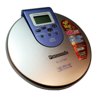
SL-CT582VGC / SL-CT582VGN / SL-CT582VGS

 Loading...