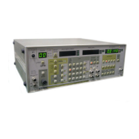
Do you have a question about the Panasonic VP-7722A and is the answer not in the manual?
| Brand | Panasonic |
|---|---|
| Model | VP-7722A |
| Category | Measuring Instruments |
| Language | English |
Details the power supply system for the digital circuit, oscillator, and analyzer.
Covers the oscillator sections A5 and A6, including amplitude control.
Discusses the preamplifier boards A7 for L and R channels and their functions.
Describes input connectors for balanced and unbalanced measurements.
Explains the operation of the input attenuator when activated by signal level.
Details the preamplifier circuit, amplification factors, and input conditioning.
Describes the average detector for signal level measurements and its data conversion.
Explains the IMD measurement circuit block diagram and its components.
Covers the 1st and 2nd notch boards for fundamental wave rejection.
Details the components and block diagram of the 1st notch filter circuit.
Lists the necessary equipment for performing adjustments and maintenance.
Details preparations required before starting adjustment procedures.
Adjustment and check procedures for the 80 MHz VCO.
Details adjustments for the oscillator board A6.
Procedure for adjusting the offset of the oscillator amplifier.
Adjustment and check procedures for the Automatic Level Controller (ALC).
Procedures for checking and adjusting the attenuator board A5.
Procedure for checking the attenuation factor of the attenuator.
Adjustments for the Preamplifier (L Channel) board A7.
Procedure to adjust the offset of the preamplifier.
Setup and adjustment procedure for the B input preattenuator.
Adjustments for the Preamplifier (R Channel) board A7.
Procedure for offset adjustment of the 2nd notch amplifier.
Adjustment procedure for the auto tuning circuit.
Procedure for adjusting the offset of the 1st notch amplifier.
Adjustment procedure for the fundamental wave rejection circuit.
Adjustment and check procedures for 80 kHz fundamental wave rejection.
Procedures for the 2nd Notch Board A9.
Adjustment procedure for the High-Pass Filter (HPF) offset.
Adjustment procedure for the PSOPHO offset.
Adjustment procedure for offset amplifier 2.
Procedures for adjusting gain and offset of average response.
Adjustment procedure for PSOPHO gain.
Procedures for the 1st Notch Board A8.
Procedure for adjusting deviation of 1 kHz 2nd harmonic.
Procedures for adjusting deviation of 100 kHz 2nd harmonic.
Procedures for the fundamental wave rejection circuit.
Adjustment procedure for the A/D Converter Board A11.
Troubleshooting flowchart for identifying issues with the VP-7722A.






 Loading...