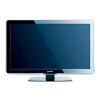
Do you have a question about the Philips 42PFL5604H/12 and is the answer not in the manual?
| Display Technology | LCD |
|---|---|
| HDMI Ports | 3 |
| Screen Format | 16:9 |
| Component Video (YPbPr/YCbCr) in | 1 |
| Number of Speakers | 2 |
| RMS Rated Power | 20 W |
| Screen Size | 42 inches |
| Audio Output | 20 W |
| Resolution | 1920 x 1080 (Full HD) |
Details electrical and product specifications for the TV model.
Outlines critical safety regulations and precautions for performing repairs.
Highlights important warnings regarding ESD, high voltage, and component handling.
Provides general notes on measurements, waveforms, and schematic conventions.
Lists and defines abbreviations used throughout the service manual.
Illustrates cable routing and management within the TV chassis.
Describes methods for positioning the TV for safe and easy servicing.
Details the procedure for removing major assemblies like the rear cover and LCD panel.
Discusses key test points and using test patterns for diagnostics.
Introduces service modes like SDM, SAM, and CSM for diagnostics and adjustments.
Explains how to activate and use Service Default Mode for consistent measurements.
Details the methods for activating and navigating the Service Alignment Mode.
Explains how to activate the Customer Service Mode (CSM) for customer support.
Explains the TV start-up sequence and protection states.
Describes service tools like ComPair for diagnostics and software upgrades.
Details how error codes are logged, their format, and relation to faults.
Explains the procedure for interpreting front LED blinks as error codes.
Describes the various software and hardware protection mechanisms in the TV.
Offers practical advice for troubleshooting and repairing common issues.
Explains how to use UART logging with HyperTerminal for fault finding.
Emphasizes checking the display option code after SSB replacement.
Provides instructions for upgrading the TV's main and stand-by software.
Specifies conditions for performing electrical alignments, including power supply and warm-up.
Details software alignments accessible via SAM, including Tuner AGC and White Point.
Explains the purpose and default value of the Tuner AGC alignment.
Details the procedure for aligning the white point and setting picture parameters.
Explains how option codes are used to configure the microprocessor and set up the TV.
Explains how to identify and order the correct SSB using 12NC and serial numbers.
Details how to view SW versions, CTN, and production codes in SAM.
Lists the software alignments available, including Tuner AGC and White Point.
Lists various options for digital broadcast, installation, and over-the-air download.
Details how to view display panel codes and select light guide options.
Introduces the Q543.3E LA chassis and its relation to the Q522.2E LA chassis.
Describes the power supply unit and its specifications.
Details the DC-DC converters used on the main board and their block diagram.
Describes the key components of the TV's front-end circuitry.
Explains the HDMI multiplexer implementation and EDID control.
Details the PNX8543's role in video and audio processing.
Describes the TCON's function and integration onto the SSB.
Explains the CI+ Conditional Access system extension.
Provides the block diagram and pin configuration for the NCP5422AD IC.
Shows the block diagram and pin configuration for the ST1S10PH IC.
Displays the block diagram and pin configuration for the LD3985M IC.
Provides the block diagram and pin configuration for the DRX3926K IC.
Shows the block diagram and pin configuration for the PNX8543 IC.
Displays the block diagram and pin configuration for the DP83816 Ethernet controller IC.
Shows the block diagram and pin configuration for the TPA3123D Class-D amplifier IC.
Provides the application schematic and pin configuration for the TPS65162RGZR IC.
Displays the block diagram and pin configuration for the BUF16821 IC.
Shows the block diagram and pin configuration for the BD8162EKV IC.
Displays the internal block diagram for the T-Con Control IC.
Illustrates the wiring connections for 32" LGD Forward Integration models.
Shows the wiring connections for 32" Sharp Forward Integration models.
Illustrates wiring for 37" LGD Forward Integration models.
Shows wiring connections for 42" LGD Forward Integration models.
Provides a high-level block diagram of the TV's video processing path.
Illustrates the audio signal flow and processing blocks.
Shows control signals and clock distribution within the TV.
Depicts the I2C communication paths between components.
Provides an overview of the various power supply lines and their sources.
Shows the circuit diagram and PWB layout for the DC/DC +3V3 +1V2 B01A SSB.
Provides the circuit diagram and PWB layout for the DC/DC +3V3 +1V2 Stand-by B01B SSB.
Shows the circuit diagram and PWB layout for the Front End B02A SSB.
Provides the circuit diagram and PWB layout for the PNX8543 Power B03A SSB.
Shows the circuit diagram and PWB layout for the PNX8543 LVDS Output B03B SSB.
Provides the circuit diagram and PWB layout for the PNX8543 Audio Amplifier B03C SSB.
Shows the circuit diagram and PWB layout for the PNX8543 Audio B03D SSB.
Provides the circuit diagram and PWB layout for the PNX8543 Analog AV B04A SSB.
Shows the circuit diagram and PWB layout for the PNX8543 SDRAM B03F SSB.
Provides the circuit diagram and PWB layout for the PNX8543 Control MIPS/Flash/PCI B03G SSB.
Shows the circuit diagram and PWB layout for the PNX8543 Stand-by Control/Debug B03H SSB.
Provides the circuit diagram and PWB layout for the Bolt-on B04A SSB.
Shows the circuit diagram and PWB layout for the Analog IO - SCART 1 & 2 B04B SSB.
Provides the circuit diagram and PWB layout for the YPbPr / Side I/O / S-video B04C SSB.
Shows the circuit diagram and PWB layout for the HDMI B05A SSB.
Provides the circuit diagram and PWB layout for the Ethernet B05B SSB.
Shows the circuit diagram and PWB layout for the PCMCIA B05C SSB.
Provides the circuit diagram and PWB layout for the Class-D B06A SSB.
Shows the circuit diagram and PWB layout for the Display Interface (Common) B07A SSB.
Provides the circuit diagram and PWB layout for the Display Supply (LGD panel) B07B SSB.
Shows the circuit diagram and PWB layout for the T-Con DC/DC (LGD panel) B09A SSB.
Provides the circuit diagram and PWB layout for the T-Con Control (LGD panel) B09B SSB.
Shows the circuit diagram and PWB layout for the T-Con Connectors (LGD panel) B09C SSB.
Provides the circuit diagram and PWB layout for the Display Supply (Sharp panel) B07B SSB.
Shows the circuit diagram and PWB layout for the T-Con DC/DC (Sharp panel) B09A SSB.
Provides the circuit diagram and PWB layout for the T-Con Control (Sharp panel) B09B SSB.
Shows the circuit diagram and PWB layout for the T-Con VCOM (Sharp panel) B09C SSB.
Provides the circuit diagram and PWB layout for the T-Con Connectors (Sharp panel) B09D SSB.
Shows the circuit diagram and PWB layout for the Display Supply (37" LGD panel) B07B SSB.
Provides the circuit diagram and PWB layout for the T-Con DC/DC (37" LGD panel) B09A SSB.
Shows the circuit diagram and PWB layout for the T-Con LG Control (37" LGD panel) B09B SSB.
Provides the circuit diagram and PWB layout for the T-Con Connectors (37" LGD panel) B09C SSB.
Explains the purpose and function of the Service Reference Protocol (SRP).
Discusses different types of signals and their representation in schematics.
Explains the SRP tool and symbols used for signal references.