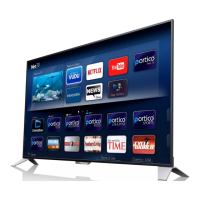
Do you have a question about the Philips 55PFL8008S/12 and is the answer not in the manual?
Details on product information, getting started, manuals, FAQs, and software.
Overview of side and rear connections for the television.
Crucial safety regulations and procedures for repairing the set.
Step-by-step instructions for removing the assembly or panel.
Explains Service Default Mode (SDM) and Service Alignment Mode (SAM).
Details the purpose and activation of SDM for pre-defined settings.
Explains CSM purpose, activation, and data dumping to USB.
Describes the start-up diagrams and conditions for various states.
Explains the error code buffer, how errors are logged, and when they are removed.
Explains the error code buffer, how errors are logged, and when they are removed.
Describes methods to clear the error buffer via SAM menu or automatically.
Explains the blinking LED procedure for Layer 1 and Layer 2 errors.
Explains the blinking LED procedure for Layer 1 and Layer 2 errors.
Details methods for activating CSM or SDM to view blinking LEDs.
Explains protections related to supplies and safety check mechanisms.
Explains protections related to supplies and safety check mechanisms.
Explains CSM activation and its data dumping mechanism to USB.
Details input power, voltage distribution, and switching regulators.
Describes how to use Hyperterminal for UART logging and interpret the output.
Step-by-step instructions for exchanging an SSB, including data upload and software upgrade.
Information on automatic and manual software upgrades.
Describes normal conditions for automatic software upgrades.
Steps to upgrade Standby software using a USB stick.
Specifies electrical adjustment conditions, including power supply and test probe requirements.
Steps for setting picture parameters and performing white point alignment.
Introduces the QFU1.2E LA chassis and its relation to the FUSION platform.
Describes power supplies as black boxes and ordering new boards.
Shows the block diagram and pinning information for the DVBT2 channel decoder IC.
Presents a comprehensive block diagram of the TV system architecture.
Illustrates the power supply lines and voltage distribution within the chassis.
Circuit diagram and PWB layout for SSB B01A, focusing on the power connector.
Detailed circuit diagram of the B01A power connector section.
Circuit diagram for the B01B Fusion power supply module.
Circuit diagram for the B01D internal USB connection.
Circuit diagram for the B02A Hybrid T/C tuner module.
Circuit diagram for the B02B satellite tuner and its diversity matrix.
Circuit diagram for the B02C DVBT2 channel decoder.
Circuit diagram for the B02D DVBS/S2 channel decoder.
Circuit diagram and PWB layout for the B03A Fusion module, showing pin assignments.
Circuit diagram and PWB layout for the B03B Fusion Umac controller and DDR3 memory interface.
Circuit diagram and PWB layout for the B03C Umac 1 DDR3 memory interface.
Circuit diagram and PWB layout for the B03D Umac 0 DDR3 memory interface.
Circuit diagram and PWB layout for the B03E Fusion module, illustrating various connections.
Circuit diagram and PWB layout for the B03F Fusion power supply.
Circuit diagram and PWB layout for the B04A control, temperature sensor, and service interface.
Circuit diagram and PWB layout for the B04B LVDS interface.
Circuit diagram and PWB layout for the B04E audio and video connections.
Circuit diagram and PWB layout for the B04F Fusion supply module.
Circuit diagram and PWB layout for the B04G backlight microcontroller.
Circuit diagram and PWB layout for the B04H eMMC storage module.
Circuit diagram and PWB layout for the B05A Class-D audio amplifier.
Circuit diagram and PWB layout for the B05C sensor board and Ambilight control.
Circuit diagram and PWB layout for the B06A HDMI connectors and related circuitry.
Circuit diagram and PWB layout for the B06B HDMI-ARC functionality.
Circuit diagram and PWB layout for the B06C external USB connectors.
Circuit diagram and PWB layout for the B06D Ethernet connector and PHY.
Circuit diagram and PWB layout for the B06E NAND flash, serial flash, and EEPROM.
Circuit diagram and PWB layout for analogue external connections.
Circuit diagram and PWB layout for the B06G DC-DC converters.
Circuit diagram and PWB layout for the B06H DC-DC converters.
Circuit diagram and PWB layout for the B06I CI conditional access module.
Circuit diagram and PWB layout for the B06J FE (Front-End) module.
Circuit diagram and PWB layout for the B06K HDMI module.
Circuit diagram and PWB layout for the B06L control, temperature sensor, and service interface.
Circuit diagram and PWB layout for the B06N headphone connector.
Circuit diagram and PWB layout for the B01A power connector on the 310431366185 SSB.
Circuit diagram and PWB layout for the B01B Fusion supply.
Circuit diagram and PWB layout for the B01D internal USB connection.
Circuit diagram and PWB layout for the B02A Hybrid T/C tuner.
Circuit diagram and PWB layout for the B02B satellite tuner.
Circuit diagram and PWB layout for the B02C DVBT2 channel decoder.
