4 - 54 - 5
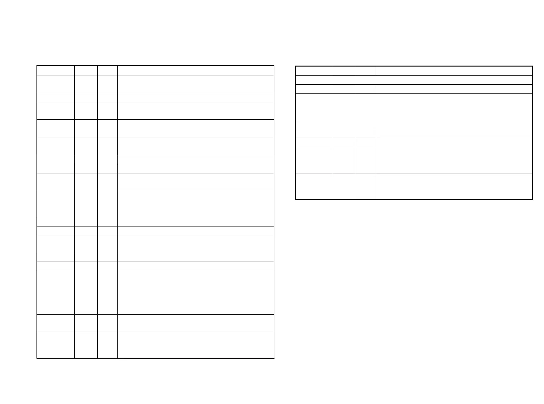
PINS DESCRIPTION OF DIGITAL VIDEO ENCODER SPCA711A
PIN FUNCTION
Mnemonic PIN No. Type Description
DATA[7:0] 21 - 28 I YCrCb pixel inputs. They are latched on the rising edge of CLK.
YCrCb input data conform to CCIR 601.
CLKOUT 29 O Pixel clock output
VSYNC 32 I/O Vertical sync input/output. VSYNC is latched/output following the rising
edge of CLK.
HSYNC 1 I/O Horizontal sync input/output. HSYNC is latched/output following the
rising edge of CLK.
MASTER 16 I Master/slave mode selection. A logical high for master mode
operation. A logical 0 for slave mode operation.
CBSWAP 15 I Cr and Cb pixel sequence configuration pin. A logic high swap the
Cr and Cb sequence.
SVIDEO 14 I SVIDEO select input pin. A logic high selects Y/C output. A logic low
selects composite video output.
SLEEP 13 I Power save mode. A logic high on this pin puts the chip into power-
down mode. This pin is equal to reset pin. An external logic high pulse
should input to the pin when power on.
MODEA 17 I Mode configuration pin.
MODEB 18 I Mode configuration pin.
CLK 19 I 27MHz crystal oscillator input. A crystal with 27MHz clock frequency can
be connected between this pin and XTALO.
XTALO 20 O Crystal oscillator output.
TEST 2 I Test pin. These pins must be connected to DGND.
VREFIN 9 I Voltage reference input. An external voltage reference must supply
typical 1.235V to this pin. A 0.1µF ceramic capacitor must be used to
de-couple this input to GND. The decoupling capacitor must be as
closed as possible to minimize the length of the load. This pin may be
connected directly to VREFOUT.
VREFOUT 8 O Voltage reference output. It generates typical 1.2V voltage reference
and may be used to drive VREFIN pin directly.
FSADJ 5 - Full-Scale adjust control pin. The Full-Scale current of D/A converters
can be adjusted by connecting a resistor (RSET) between this pin and
ground.
Mnemonic PIN No. Type Description
VAA 7 - Analog power pin
AGND 3,12 - Analog ground pin
COMP 6 - Compensation pin. A 0.1µF ceramic capacitor must be used to bypass
this pin to VAA. The lead length must be kept as short as possible to
avoid noise.
VBIAS 10 - DAC bias voltage. Potential normally 0.7V less than COMP.
VDD 31 - Digital power pin
DGND 30 - Digital ground pin
CVBSY 4 O Composite/Luminance output. This is a high-impedance current source
output. The output format can be selected by the PAL pin. The
CVBSY can drive a 37.5 1 load.
CVBSC 11 O Composite/Chroma output. This is a high impedance current source
Output. The output format can be selected by the PAL pin. The pin
can drive a 37.5 1 load.
PINS DESCRIPTION OF DIGITAL VIDEO ENCODER SPCA711A
PIN FUNCTION