Ill
3.2.
1.6. Delay
-line
driver
bases
of
the
output
transistors
Vb02,
V504
of
the
shunt-senes
feedback
amplifier
and
each
normally
draws
10
mA
from
the
current
source
of V501,
V503.
When
the
channel
is
switched
off by
the
diode-gate
network,
the
signal
transistors
are
blocked
and
the
alternative
transistors
are
switched
on
so
that
they
now
draw
20
mA
current
from
the
-Ml
,4
V rail
via
resistors R502,
R501,
R508,
R507.
Similarly,
the
collector
outputs
from
D303
of the
channel
B
intermediate
amplifier
are
also
coupled
to
the
bases
of V502,
V504.
In
the ADD
position,
with
both
the A
and
B channels
switched in,
20 mA is
fed
to V224
and V322
and,
similarly,
20 mA
to V222, V324.
Since
the alternative
transistors
in D203
and D303
are
now
switched
off,
only
10
mA
is drawn via
the R501
and R507.
The
table shows
the
current
distribution
in
the
stage for the
various
operating
modes.
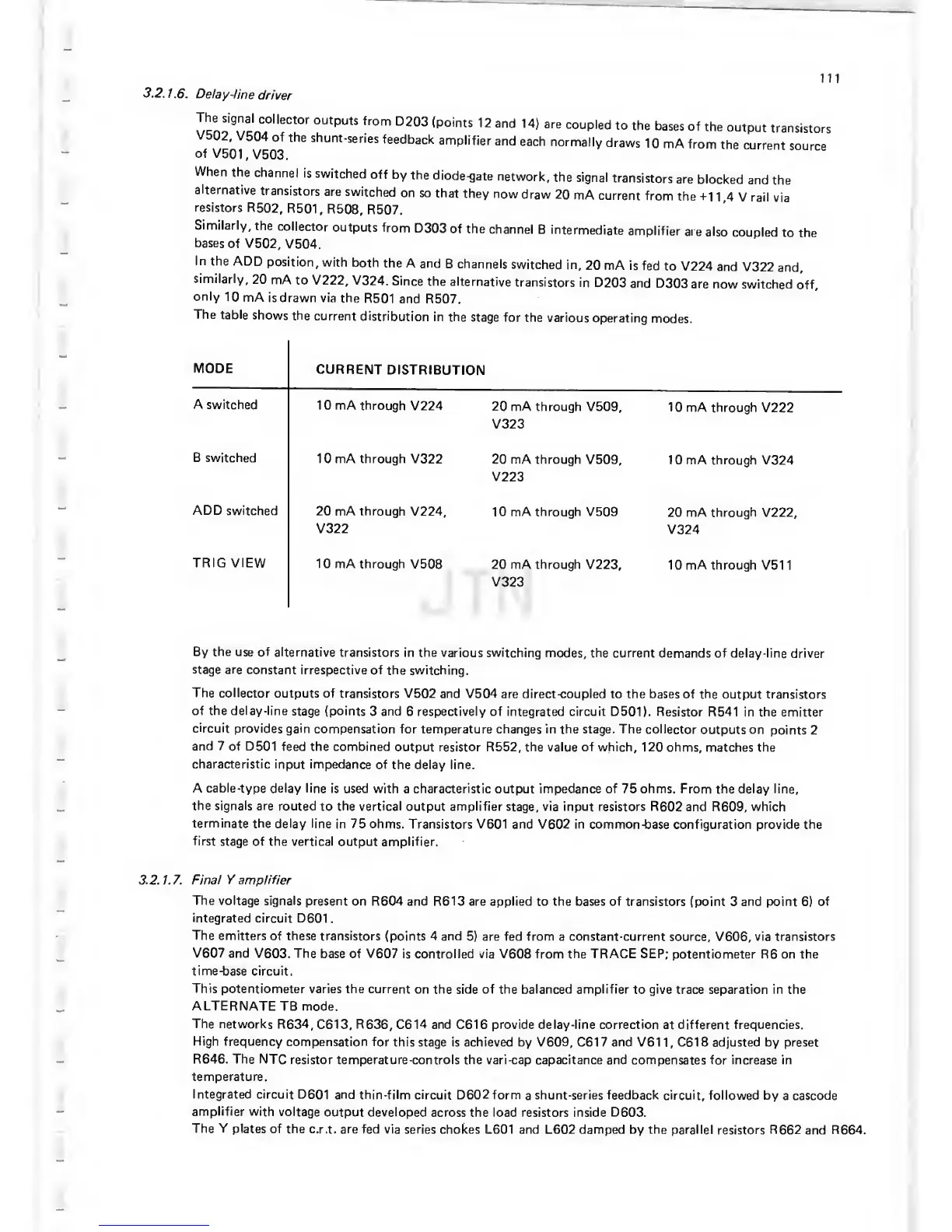
MODE
CURRENT
DISTRIBUTION
-
A
switched
1 0 mA
through
V224
20 mA through
V509,
V323
1
0 mA through
V222
-
B switched
1
0
mA
through V322
20 mA through V509,
V223
1
0
mA
through V324
—
ADD
switched
20 mA through
V224,
V322
10 mA through V509
20 mA through V222,
V324
—
TRIG VIEW
1 0 mA through V508
20 mA through V223,
V323
10
mA through
V511
By the
use of alternative
transistors in the various switching
modes, the current
demands of delay -line driver
stage are
constant
irrespective of
the
switching.
The collector
outputs of
transistors
V502
and V504
are direct -coupled to the bases of
the output transistors
of
the delay -line
stage (points
3
and
6 respectively of integrated circuit D501).
Resistor
R541
in
the
emitter
circuit
provides
gain compensation for
temperature changes in the stage. The collector
outputs on
points 2
and 7 of D501
feed the combined
output resistor
R552,
the value
of
which, 1
20 ohms, matches the
characteristic
input
impedance
of the delay line.
A
cable-type delay line
is
used
with
a
characteristic
output impedance of 75 ohms. From
the
delay line,
the signals are
routed
to
the vertical
output
amplifier
stage,
via input resistors R602
and R609, which
terminate
the
delay
line
in 75 ohms.
Transistors
V601
and V602 in common
-base
configuration
provide the
first
stage
of
the vertical output amplifier.
3. 2.
1.7.
Final Y amplifier
The
voltage signals
present on R604
and
R613 are applied
to the bases of transistors (point
3
and
fjoint
6)
of
integrated
circuit D601
.
The
emitters of these transistors
(points 4 and
5)
are fed from
a
constant-current
source, V606, via transistors
V607 and
V603. The
base of
V607
is controlled via V608 from the TRACE SEP;
potentiometer R6 on the
time-base circuit.
This
potentiometer varies the current
on the side
of
the balanced amplifier
to
give
trace separation in the
ALTERNATE
TB mode.
The networks R634,
C613,
R636,
C614 and C616 provide delay-line correction
at
different frequencies.
High
frequency
compensation for
this stage is achieved by V609, C617 and V61
1,
C618 adjusted by preset
R646.
The NTC
resistor temperature-controls
the vari-cap capacitance and compensates for increase in
temperature.
Integrated
circuit D601
and thin-film
circuit D602form
a
shunt-series feedback
circuit, followed by
a
cascode
amplifier with
voltage
output developed
across the load resistors inside D603.
The
Y
plates of the
c.r.t. are fed via series chokes
L601 and L602 damped by the
parallel resistors
R662
and
R664.
 Loading...