112
Together
with
the
capacitance of
the c.r.t.
plates, this forms
a series resonant
circuit
to
lift
the gain
at the high
frequency
end
of
the bandwidth.
Preset R654
provides
a
measure of
gain
adjustment
(20 %
approx.) to allow
for
different
c.r.t. sensitivities.
It controls
the
quiescent
current
of the
diodes
and thus the
gain of
the D601
amplifier
stage.
Any
unbalance
in
the
c.r.t. deflection
plates
can be
corrected for
by the line
centring
preset R658,
which
provides
a compensating
current
for one side of
the
balanced
output stage.
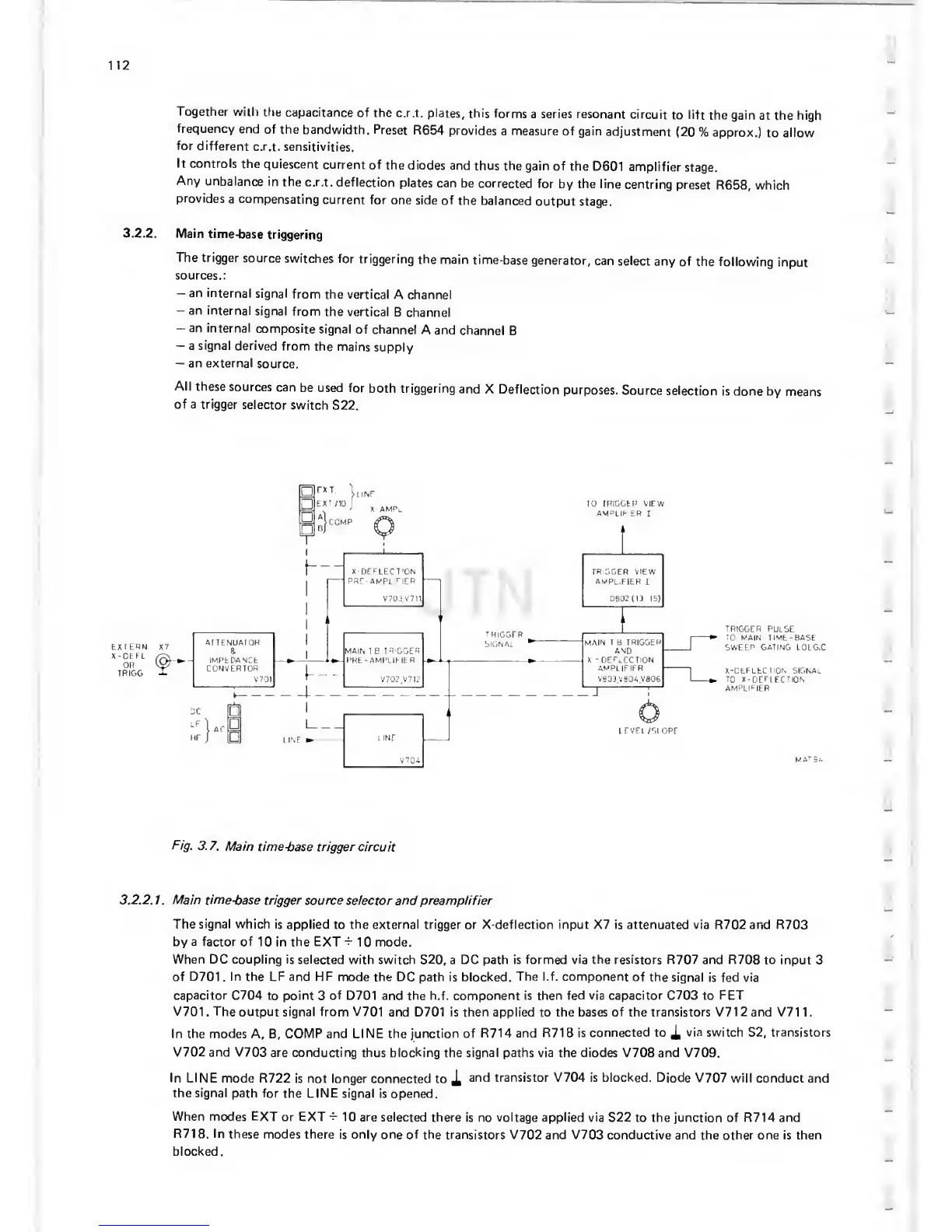
3.2.2.
Main
time-base
triggering
The
trigger
source
switches
for
triggering
the
main time-base
generator, can
selea
any
of the
following
input
sources.;
—
an
internal
signal
from
the vertical
A channel
—
an
internal
signal
from
the vertical
B
channel
—
an internal
composite
signal
of
channel
A and
channel
B
—
a
signal
derived
from
the mains
supply
—
an
external
source.
All these
sources
can
be used for
both triggering
and X
Deflection
purposes.
Source
selection
is done by
means
of
a trigger
selector
switch
S22.
tXIEHN
X-DEFL
OR
TRIG6
TRIGGER PULSE
ro WAIN TIME
-BASE
SWEEP GATING
LOLG.C
X-OEFLECnON SIGNAL
TO
X-DEFIFCTION
AMPLIFIER
Fig.
3.
7. Main time-base
trigger circuit
3.2.2.
1.
Main
time-base trigger source
selector and
preamplifier
The
signal which
is
applied to
the
external trigger or X-deflection input X7 is attenuated via
R702 and
R703
by a factor of 10 in the EXT
-1-
10 mode.
When DC coupling is
selected with switch
S20, a
DC path is formed via
the
resistors R707 and R708 to
input 3
of D701
.
In the LF
and
HF
mode the DC path is blocked.
The
l.f. component
of the
signal
is
fed via
capacitor
C704 to point
3
of
D701
and
the h.f. component is then fed
via capacitor
C703 to
FET
V701
.
The
output signal from V701
and D701 is then applied to the bases of the transistors V71
2
and V71 1
.
In the modes
A, B,
COMP and LINE the junction of
R714 and
R718 is
connected to
X
via switch
S2,
transistors
V702 and V703
are conducting thus blocking
the signal paths via the diodes V708 and V709.
In LINE
mode R722
is not longer connected
to
X
transistor V704 is blocked.
Diode V707
will conduct and
the signal
path for the LINE
signal is opened.
When
modes EXT
or EXT
-r
10 are
selected there
is no
voltage applied via
S22 to the junction of R714 and
R718. In
these modes
there is only one
of the transistors V702
and
V703
conductive and the other one is then
blocked.
 Loading...