12
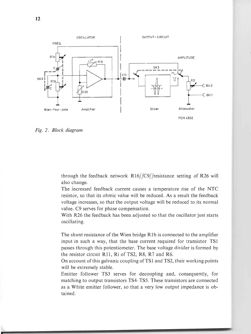
OSCILLATOR
OUTPUT - CIRC UIT
FREQ.
,------------------,
Wien-
four-pole
Amptifier
AMPLITUDE
SK3
F========~
~7
"
...
,n
,,,,,
BU2
""
~if
fi
~----<"'BUl
Slicer
A
ttenuator
Fig. 2. Block diagram
through the feedback network
Rl6j
jC9j
jresistance setting
of
R26 will
also change.
The increased feedback current causes a temperature rise
of
the
NTC
resistor, so
that
its ohmic value will
be
reduced. As a result the feedback
voltage increases, so
that
the
output
voltage will be reduced to its normal
value. C9 serves for phase compensation.
With R26 the feedback has been adjusted so that the oscillator just starts
oscillating.
The shunt resistance
of
the Wien bridge
Rl
b
is
connected to the amplifier
input
in
such
away,
that
the base current required for transistor
TSl
passes through this potentiometer. The base voltage divider is formed
by
the resistor circuit
Rll,
Ri
of
TS2, R8, R7 and R6.
On
account
of
this galvanic coupling
ofTSl
and TS2, their working points
will be extremely stable.
Emitter follower TS3 serves for decoupJing and, consequently, for
matching to
output
transistors TS4--TSS. These transistors are connected
as a White emitter follower, so
that
a very low
output
impedance
is
ob-
tained.