Circuit Descriptions, Abbreviation List, and IC Data Sheets
EN 129Q529.1A LA 9.
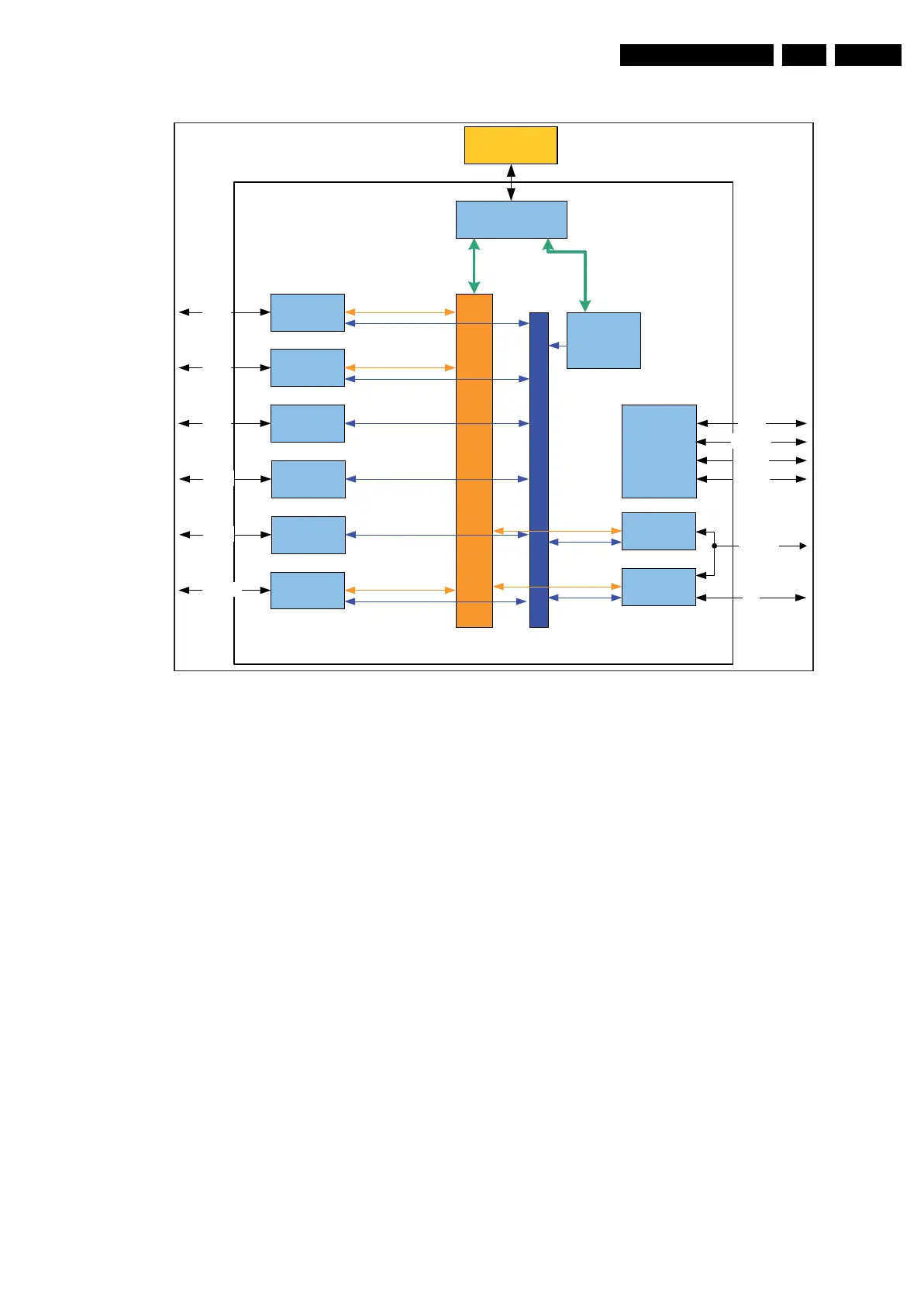
Figure 9-8 Control and compute subsystem
The Control and compute subsystem consists of the main
processor, control peripherals and the memory system.
The MIPS 4KEc is a 32-bit MIPS RISC core. It has direct
access to connectivity peripherals to support system features
via PCI, I
2
C, UART or General Purpose I/O. A JTAG interface
provides processor software debug capabilities.
The Memory Control Unit (MCU) is a 32-bit DDR2 SDRAM
interface supporting DDR2-533 with an address range of
128 MB (max.).
The PCI/XIO interface supports PCI Rev2.2 and can be used
to access 8/16-bit external NAND-Flash memory.
9.6 Back-end
Refer to figure “9-1 Architecture of TV522/92 platform (AP
region)” earlier in this chapter for details. Refer also to block
diagram B05.
In HD sets (50 / 100 Hz), the output signal coming from the
PNX85xx is fed to the PNX5100. The PNX5100 also generates
the pulse-width modulated signal needed for the “Dimming
Backlight” feature, which ensures additional motion sharpness.
As some displays require an analogue signal to switch the
LCD, a multiplexer is added to transform the pulse width
modulated signal. An additional signal, coming from the
PNX85xx, makes the selection between analogue and pulse-
width modulation, depending on which display is used.
Scanning back light displays require an analogue signal, and
all other displays a pulse-width modulated.
Refer to figure “9-9 PNX5100 Detailed Video Block diagram”.
H_16770_126.eps
130707
D
C
S
-
N
e
t
w
o
r
k
I2C-3
MCU
D
M
A
B
u
s
PNX85xx
DDR2-SDRAM
I2C-DMA3
I2C-2 I2C-DMA2
PCI/XIO
PCI/XIO
2-wire UART1
2-wire UART2
MIPS
MTI-4KeC
System
Controller
80C51
I2C-4
UART-3
PWM’s
GPIO’s
CAI
CA
I2C-1 I2C-Slave
E-JTAG
E-JTAG
DMA