Page 2.1
PROGRAMMABLE POTENTIOMETER MODULE 40-296
pickering
SECTION 2 - TECHNICAL DESCRIPTION
SECTION 2 - TECHNICAL DESCRIPTION
FUNCTIONAL DESCRIPTION
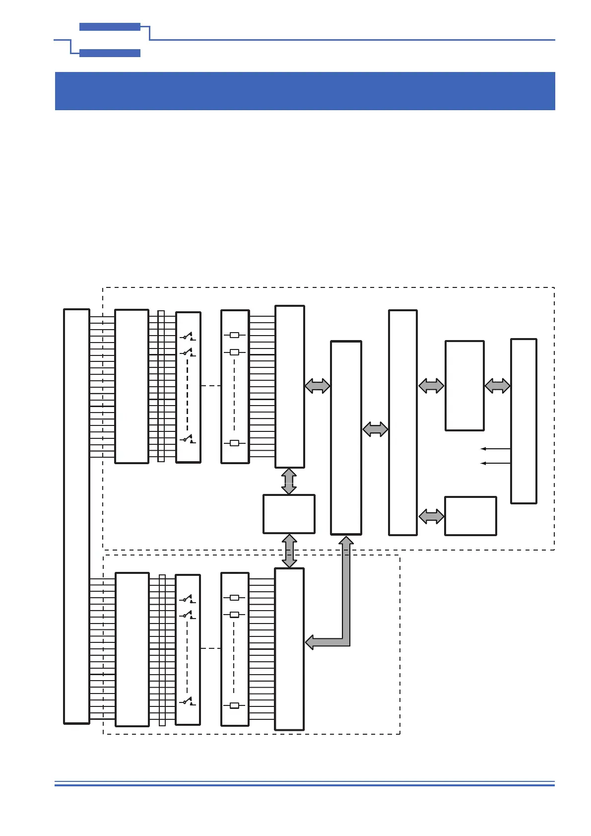
A functional block diagram is provided in Figure 2.1. Figures 2.2 and 2.3 provide examples of potentiometer chain
schematic diagrams for the 40-296-121-9/8 version of the card. The Programmable Potentiometer Card is powered
by +5V inputs via the PXI connector, J1. The interface to the user test equipment is via the front panel mounted
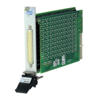
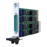
37-pin D-type connector, J2. The module comprises two PCBs populated with resistor chains which are switched
via single pole relays. The two PCBs are connected via a plug and socket connector arrangement. The relays
are energised via control signals from relay drivers which are addressed by PCI bridge U1, via the control logic
comprising U3 to U6, to output the required signal. Module conguration is determined by hardwired links and data
stored in EEPROM U7 PCI Bridge U1 is congured by EEPROM U2.
Each resistor chain includes an offset resistor that can be used to set the minimum resistance value.
Figure 2.1 - Programmable Potentiometer Module 40-296: Functional Block Diagram
37-PIN
D TYPE
CONNECTOR
J2
MODULE
CONFIGURATION
U7
PCI
BRIDGE
U1
PCI BRIDGE
CONFIGURATION
U2
TERMINATING
RESISTORS
R3 TO R14
COMPACT PCI
BUS
CONNECTOR
J1
+5V
0V
RELAY
COILS
RELAY
CONTACTS
CONTROL
LOGIC
U3, U4,
U5, U6
RELAY
COILS
RELAY
CONTACTS
MOTHERBOARD
DAUGHTERBOARD
RELAY
DRIVERS
U8 TO
U15
RELAY
DRIVERS
U1 TO
U5
RESISTOR
CHAINS
RESISTOR
CHAINS
LINKS
LINKS