Do you have a question about the Pioneer BDP-LX55 and is the answer not in the manual?
Covers safety precautions, warnings, leakage current checks, and product safety notices.
Flowchart for diagnosing problems with VFD display and buttons not working.
Flowcharts for diagnosing no audio output and remote control malfunctions.
Flowchart for diagnosing problems with reading discs or opening the disc door.
Flowchart for diagnosing and resolving issues related to the absence of video display.
Flowchart for diagnosing problems when the unit cannot connect to the network.
Flowchart for diagnosing no audio output specifically from the Sub HDMI connection.
Flowchart for diagnosing no video output specifically from the Main HDMI connection.
Instructions for entering Service Mode and descriptions of its menu items.
Detailed steps for performing FA mode to adjust pick-up and verify disc playback.
Necessary adjustment points after replacement and procedure for firmware update.
Schematic diagram of the main board's power source circuit, including regulators.
Schematic showing DC-DC converters and voltage regulators on the main board.
Schematic diagram of DDR memory interface connections (Part 1).
Schematic diagram of DDR memory pin assignments and connections (Part 2).
Schematic diagram of DDR2 memory interface connections (Part 1).
Schematic diagram of DDR2 memory pin assignments and connections (Part 2).
Schematic diagram of the HDMI output circuitry, including DDC and CEC.
Schematic diagram of HDMI port connections, CEC circuit, and VCXO circuit.
Schematic diagram of flash memory, USB, Ethernet, and serial interface circuits.
Schematic diagram showing NAND flash, USB, and serial interface connections.
Schematic diagram of the VFD and IR receiver circuits.
Schematic diagram for VFD control, IR receiver, and RS232 debug jack.
Schematic diagram of the Audio Digital-to-Analog Converter (DAC) circuit.
Schematic diagram showing audio mute circuits and power control for audio DAC.
| Storage media type | Not available |
|---|---|
| Built-in storage media | No |
| Total storage capacity | - GB |
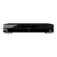
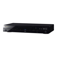
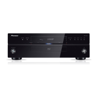
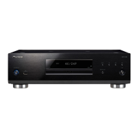
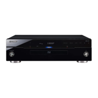
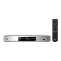
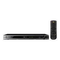
| Product color | Black |
| Supported radio bands | - |
| Image formats supported | JPG |
| Video formats supported | 3GP, AVI, DIVX, FLV, M2TS, M4V, MOV, MPEG2, MPEG4, TS, WMV |
| Analog signal format system | NTSC J, PAL |
| Audio decoders | Dolby Digital, Dolby Digital EX, Dolby Digital Plus, Dolby TrueHD, DTS, DTS 96/24, DTS-ES |
| Audio output channels | 2.0 channels |
| DC-in jack | Yes |
| Composite video out | 1 |
| USB 2.0 ports quantity | 2 |
| USB 3.2 Gen 1 (3.1 Gen 1) Type-A ports quantity | 0 |
| AC input voltage | 200 - 240 V |
| AC input frequency | 50 - 60 Hz |
| Power consumption (standby) | 0.3 W |
| Power consumption (typical) | 25 W |
| Disc types supported | BD-R, BD-RE, BD-ROM, CD-R, CD-RW, DVD+R, DVD+RW, DVD-R, DVD-RW |
| Depth | 93 mm |
|---|---|
| Width | 435 mm |
| Height | 252 mm |
| Weight | 3500 g |