98
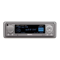
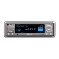
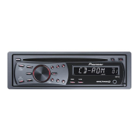
DEX-P1R,DEH-P946,DEX-P1
7. GENERAL INFORMATION
7.1 PARTS
7.1.1 IC
UPD63702AGF
BA6797FM
LC89170M
BA05SFP
LB1930M
PM2006A
PD6191A
PD8034A
PD4908A
PD4906A
PD4931A
PD0236AM
PD6237B
SED1540F0A
SED1526F0A
PD5445A
AK7712AVT
GGC1325(M5M51016BTP-70LL)
TC7S08FU
PE2001AF
PM0017AM
NJM4580M
- Pin Functions (UPD63702AGF)
Pin No. Pin Name I/O Function and Operation
1 D.VDD Supplies current of positive voltage to the logic circuits
2 rst I System reset input pin
3 AO I Microcomputer interface
AO="L": stb active and set to address register
AO="H": stb active and set to parameter
4 stb I Signal to latch serial data within the LSI
5 sck I Clock input pin to input and output serial data
6 SO O Outputs serial data and status signal
7 SI I Serial data input pin
8 D.GND Logic circuit GND
9 X.GND Crystal oscillation circuit GND
10 XTAL I Crystal oscillator connection pin
11 xtal O Crystal oscillator connection pin
12 X.VDD Supplies current of positive voltage to the crystal oscillation circuit
13 DA.VDD Supplies current of positive voltage to the D/A converter
14 R+ O Right channel analog audio data output pin
15 R- O Right channel analog audio data output pin
16,17 DA.GND D/A converter GND
18 L- O Left channel analog audio data output pin
19 L+ O Left channel analog audio data output pin
20 DA.VDD Supplies current of positive voltage to the D/A converter
21 D.VDD Supplies current of positive voltage to logic circuit
22 FLAG O Flag output pin to indicate that audio data currently being output consists of
noncorrectable data
23 WDCK O Pin to output double the frequency of LRCK
24 C16M O Pin to output the clock
25 EMPH O Output pin for the pre-emphasis data in the sub-Q code
26 DIN I Input pin for serial audio data
27 DOUT O Output pin for the serial audio data
28 SCKO O Output pin for the clock for the serial audio data
29 LRCK O Signals to distinguish the right and left channels of the audio data output
from DOUT. Frequency is 44.1kHz at 50% duty at normal regeneration
30 TX O Output pin for the digital audio interface data
31 CTLV I Oscillation control pin for high-frequency clock generation VCO used for the
digital PLL upon regeneration at fast speed of 2- or 4-fold
32 POUT O Output point for phase comparison
33 D.GND GND for the logic circuit
34 VCO I Input pin for the inverter
35 vco O Output pin for the inverter
36 D.VDD Supplies current of positive voltage to the logic circuit
37 PLCK O Pin for monitoring the bit clock
 Loading...