EasyManua.ls Logo

Pioneer PD-S507 Service Manual

Pioneer PD-S507
39 pages
To Next Page IconTo Next Page
Page #1 background imageLoading...
Page #1 background image
ORDER NO.
PIONEER ELECTRONIC CORPORATION 4-1, Meguro 1-Chome, Meguro-ku, Tokyo 153-8654, Japan
PIONEER ELECTRONICS SERVICE, INC. P.O. Box 1760, Long Beach, CA 90801-1760, U.S.A.
PIONEER ELECTRONIC (EUROPE) N.V. Haven 1087, Keetberglaan 1, 9120 Melsele, Belgium
PIONEER ELECTRONICS ASIACENTRE PTE. LTD. 501 Orchard Road, #10-00 Wheelock Place, Singapore 238880
PIONEER ELECTRONIC CORPORATION 1998
MYXK AC220–230V
MVXK AC220–230V
COMPACT DISC PLAYER
RRV2034
T–ZZR OCT. 1998 Printed in Japan
PD-S507
CONTENTS
1. SAFETY INFORMATION.................................... 2
2. EXPLODED VIEWS AND PARTS LIST ............. 3
3. SCHEMATIC DIAGRAM................................... 10
4. PCB CONNECTION DIAGRAM ....................... 17
5. PCB PARTS LIST ............................................. 24
6. ADJUSTMENT.................................................. 27
7. GENERAL INFORMATION .............................. 35
7.1 IC................................................................ 35
7.2 DISPLAY ....................................................36
7.3 BLOCK DIAGRAM ..................................... 37
8. PANEL FACILITIES AND SPECIFICATIONS
................................................................... 38
THIS MANUAL IS APPLICABLE TO THE FOLLOWING MODEL
(
S
)
AND TYPE
(
S
)
.
Remarks
Type
Model
PD-S507
Power Requirement
Question and Answer IconNeed help?

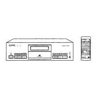
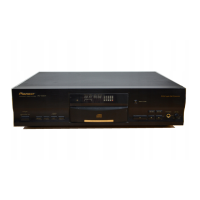
Do you have a question about the Pioneer PD-S507 and is the answer not in the manual?
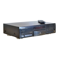
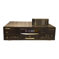
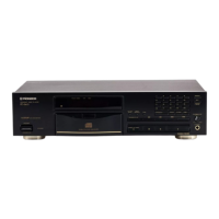
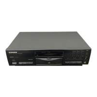
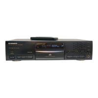
Pioneer PD-S507 Specifications

General IconGeneral
TypeCD Player
Disc formatsCD
Channels2
Frequency Response2 Hz to 20 kHz
Output Level2 V
Line output1 x RCA
Digital outputsCoaxial

Summary

SAFETY INFORMATION

Safety Warnings and Laser Precautions

Details laser safety, interlock mechanisms, and warning labels.

SCHEMATIC DIAGRAM

Overall Schematic Diagram

Comprehensive block diagram showing interconnections between major assemblies.

Main and Coaxial Output Board Schematics

Detailed schematics for the main and coaxial output assemblies.

Power, Switch, and Mode Board Schematics

Schematics for power, switch, and mode board assemblies.

Main Board Waveforms

Visual representations of key signal waveforms on the main board.

PCB PARTS LIST

ADJUSTMENT

Adjustment Procedures

Step-by-step guide for various adjustments including focus, tracking, and RF levels.

GENERAL INFORMATION

System Block Diagram

Overall system block diagram showing major functional units and interconnections.

Related product manuals