EasyManua.ls Logo

Pioneer VSX-430-K Service Manual

Pioneer VSX-430-K
31 pages
To Next Page IconTo Next Page
Page #1 background imageLoading...
Page #1 background image
ORDER NO.
PIONEER ELECTRONICS (USA) INC. P.O. Box 1760, Long Beach, CA 90801-1760, U.S.A.
PIONEER EUROPE NV Haven 1087, Keetberglaan 1, 9120 Melsele, Belgium
PIONEER ELECTRONICS ASIACENTRE PTE. LTD. 253 Alexandra Road, #04-01, Singapore 159936
2015
1-1, Shin-ogura, Saiwai-ku, Kawasaki-shi, Kanagawa 212-0031, Japan
2015 Printed in Japan
VSX-530-K
RRV4598
AV Receiver
VSX-530-K
VSX-430-K
THIS MANUAL IS APPLICABLE TO THE FOLLOWING MODEL(S) AND TYPE(S).
This service manual should be used together with the following manual(s).
For SPECIFICATIONS and PANEL FACILITIES, refer to the operating instructions.
Model Type Power Requirement Remarks
VSX-530-K CUXEVSM AC 120 V
VSX-430-K SYXEV8 AC 220 V to 230 V
Model No. Order No. Remarks
VSX-523-K RRV4418 VSX-523-K/CUXESM
K-ZZZ JULY

Other manuals for Pioneer VSX-430-K

Question and Answer IconNeed help?

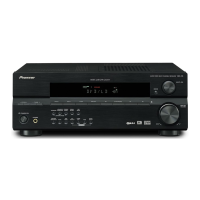
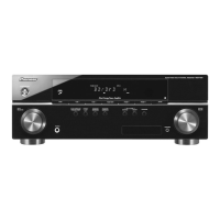
Do you have a question about the Pioneer VSX-430-K and is the answer not in the manual?

Pioneer VSX-430-K Specifications

General IconGeneral
Channels5.1
HDMI Inputs4
HDMI Outputs1
4K Ultra HD Pass-throughYes
3D ReadyYes
Audio Return Channel (ARC)Yes
Dolby TrueHDYes
DTS-HD Master AudioYes
AM/FM TunerYes
MCACC Auto Room TuningYes
Total Harmonic Distortion0.08%
Signal-to-Noise Ratio98 dB
USB Port1 (Front)
BluetoothNo
Input Sensitivity/Impedance200 mV / 47 kΩ
Dimensions (W x H x D)435 x 168 x 315.5 mm
Weight17.9 lbs (8.1 kg)

Summary

EXPLODED VIEWS AND PARTS LIST

EXTERIOR SECTION OVERVIEW

MISCELLANEOUS PARTS CONTRAST

TROUBLESHOOTING GUIDE

NO POWER DIAGNOSIS FLOWCHART

Provides a flowchart for troubleshooting "No Power" issues.

PROTECTION CIRCUITRY

OVERLOAD AND DC PROTECTION CIRCUIT

Details circuits for overload and DC protection.

TEMPERATURE PROTECTION CIRCUIT

Explains thermal protection circuits for various channels.

BLUETOOTH PAIRING PROCEDURE

SCHEMATIC DIAGRAMS

MAIN ASSY SCHEMATIC (PART 1/2)

Schematic diagram for the Main Assy, part 1 of 2.

MAIN ASSY SCHEMATIC (PART 2/2)

Schematic diagram for the Main Assy, part 2 of 2.

D-MAIN ASSY SCHEMATIC (PART 1/4)

Schematic diagram for the D-MAIN Assy, part 1 of 4.

D-MAIN ASSY SCHEMATIC (PART 2/4)

Schematic diagram for the D-MAIN Assy, part 2 of 4.

D-MAIN ASSY SCHEMATIC (PART 3/4)

Schematic diagram for the D-MAIN Assy, part 3 of 4.

PCB CONNECTION DIAGRAMS

Related product manuals