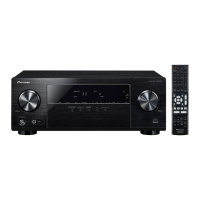
Do you have a question about the Pioneer VSX-505RDS and is the answer not in the manual?
Diagram showing the removal of the top casing of the receiver unit.
Diagram illustrating the removal of the amplifier assembly.
Diagram showing the removal of the mother assembly.
Diagram illustrating the removal of the FL and UCOM assembly.
Details on packing cases and operating instructions for different models.
List of parts for the VSX-505RDS/HVXK model, including diagrams.
Comparison of parts for VSX-505RDS/HVXK and VSX-405RDS models.
Detailed parts list for the front and rear panels of VSX-505RDS/HVXK.
Comparison of exterior parts for VSX-505RDS/HVXK and VSX-405RDS models.
Detailed parts list for the exterior components of VSX-505RDS/HVXK.
List of components for the power block section of the receiver.
Comprehensive schematic diagram of the entire receiver unit.
Schematic diagram for the second part of the mother assembly.
Schematic diagram for the surround sound processing block.
Schematic of the RDS detector circuit.
Schematic of the FL and UCOM assembly.
Schematic of the ST. IND. assembly.
Schematic for speaker switch and headphone assembly.
Schematic diagram for the video assembly.
Schematic diagram for the transformer assembly.
Schematic diagram for the regulator assembly.
Schematic diagram for the tuner section of the receiver.
Schematic of the 4-chain F.E module for the tuner.
Schematic for the right channel power amplifier.
Schematic for the center channel power amplifier.
Schematic for the left channel power amplifier.
Schematic of the overload detection circuit.
Schematic diagram for the volume control assembly.
Schematic diagram for the front speaker assembly.
Overview of all PCB assemblies and their part numbers.
Comparison of PCB assemblies for different models.
Detailed list of semiconductor, capacitor, and resistor parts.
Procedures and specifications for adjusting the FM tuner.
Procedures and specifications for adjusting the AM (MW) tuner.
Block diagram and pin function details for the NJW1102FG1 IC.
Visual layout of the NJU9702D IC pins and their functions.
Functional block diagram of the NJU9702D digital delay IC.
Pin assignments for the FL display and UCOM Assy.
Grid assignments for the FL display segments.
Anode assignments for the FL display segments.
Exploded view and parts list for the remote control unit.
List of semiconductor components on the remote control PCB.
List of capacitor components on the remote control PCB.
List of resistor components on the remote control PCB.
List of other components on the remote control PCB.
Information on switches and their functions in the remote control.
Information on viewing perspectives and PCB construction for diagrams.
Description of the power standby/on switch and indicator.
Function of the SFC mode button.
Function of the Dolby Pro Logic button.
Function of the loudness button for low volume listening.
Buttons for selecting audio input sources like PHONO, TUNER, CD.
Control for adjusting volume from all speakers simultaneously.
Jack for connecting headphones.
Buttons to select speaker output (A or B terminals).
Button for manual station name input or program type search.
Button to reduce distortion on strong FM signals.
Indicator for EON information and automatic station tracking.
Button for frequency preset mode and character registration.
Explanation of the display section indicators and character display.
Button to switch between preset memory classes.
Button to switch between FM and AM reception bands.
Buttons for scanning frequencies and selecting characters.
Buttons for changing station presets.
Control for adjusting low-frequency levels.
Control for adjusting high-frequency levels.
Control for adjusting left/right speaker volume balance.
Technical specifications for the amplifier section, including power output.
Technical specifications for the FM tuner, including sensitivity and S/N ratio.
Technical specifications for the AM tuner, including sensitivity and selectivity.
Specifications for power requirements, consumption, dimensions, and weight.
List of parts included with the receiver unit.