EasyManua.ls Logo

Pioneer VSX-908RDS Service Manual

Pioneer VSX-908RDS
100 pages
To Next Page IconTo Next Page
Page #1 background imageLoading...
Page #1 background image
ORDER NO.
PIONEER CORPORATION 4-1, Meguro 1-Chome, Meguro-ku, Tokyo 153-8654, Japan
PIONEER ELECTRONICS SERVICE, INC. P.O. Box 1760, Long Beach, CA 90801-1760, U.S.A.
PIONEER ELECTRONIC (EUROPE) N.V. Haven 1087, Keetberglaan 1, 9120 Melsele, Belgium
PIONEER ELECTRONICS ASIACENTRE PTE. LTD. 253 Alexandra Road, #04-01, Singapore 159936
PIONEER CORPORATION 1999
c
VSX-908RDS
RRV2166
1. SAFETY INFORMATION
......................................
2
2. EXPLODED VIEWS AND PARTS LIST
...............
3
3. BLOCK DIAGRAM AND SCHEMATIC DIAGRAM
...
10
4. PCB CONNECTION DIAGRAM
.........................
48
5. PCB PARTS LIST
...............................................
71
6. ADJUSTMENT
....................................................
79
CONTENTS
7. GENERAL INFORMATION
................................
80
7.1 DISASSEMBLY
............................................
80
7.2 PARTS
..........................................................
82
7.2.1 IC
............................................................
82
7.2.2 DISPLAY
.................................................
86
7.3 REMOTE CONTROL UNIT
..........................
88
8. PANEL FACILITIES AND SPECIFICATIONS
.......
93
T – ZZK JULY 1999 Printed in Japan
VSX-908RDS-G
AUDIO/VIDEO MULTI-CHANNEL RECEIVER
STANDBY/ON
DSP
MODE
STANDBY
AUDIO/VIDEO MULTI-CHANNEL RECEIVER
STEREO
THX CINEMA ADVANCED STANDARD
/DTS
MPEG
OFF _ON
EON
MODE
INPUT
SELECTOR
MASTER
VOLUME
FL
DIMMER
DOWN UP
Type
Model
Power Requirement
The voltage can be converted by the
VSX-908RDS VSX-908RDS-G following method.
HY/EW AC220-230V AC240V,
HY/GR AC220-230V AC240V,
HV AC230V AC240V,
HY AC220-230V AC240V,
THIS MANUAL IS APPLICABLE TO THE FOLLOWING MODEL(S) AND TYPE(S).
: Alter the wiring of the Power-supply block at the primary winding of Power-transformer referring to the "Line Voltage Selection" described
in Service Manual.
w
w
w
.
x
i
a
o
y
u
1
6
3
.
c
o
m
Q
Q
3
7
6
3
1
5
1
5
0
9
9
2
8
9
4
2
9
8
T
E
L
1
3
9
4
2
2
9
6
5
1
3
9
9
2
8
9
4
2
9
8
0
5
1
5
1
3
6
7
3
Q
Q
TEL 13942296513 QQ 376315150 892498299
http://www.xiaoyu163.com
Question and Answer IconNeed help?

Do you have a question about the Pioneer VSX-908RDS and is the answer not in the manual?

Pioneer VSX-908RDS Specifications

General IconGeneral
Total Harmonic Distortion (THD)0.08%
Surround SoundDolby Pro Logic
Power Output (per channel)80W
Frequency Response10Hz - 100kHz
Audio Inputs5

Summary

SAFETY INFORMATION

SAFETY PRECAUTIONS

Essential safety checks and notices for technicians and users.

LEAKAGE CURRENT CHECK

Procedure to measure leakage current to ensure user safety.

PRODUCT SAFETY NOTICE

Important notice regarding product safety characteristics and replacement parts.

EXPLODED VIEWS AND PARTS LIST

2.1 PACKING

Lists parts related to product packaging.

2.2 EXTERIOR

PCB layout and component details for the exterior section.

2.3 HEAT SINK SECTION

PCB layout and component details for the heat sink section.

2.4 FRONT PANEL SECTION

PCB layout and component details for the front panel section.

BLOCK DIAGRAM AND SCHEMATIC DIAGRAM

3.1 BLOCK DIAGRAM

High-level system overview of audio/video signal flow.

3.2 OVERALL WIRING CONNECTION DIAGRAM

Illustrates interconnections between major assemblies and connectors.

3.3 EXTERNAL IN, A-PINJACK and CONNECTION ASSYS

Diagrams for external input, A-Pinjack, and connection assemblies.

3.4 MAIN CONTROL ASSY (1/3)

Part 1 of the main control assembly PCB layout and component details.

3.5 MAIN CONTROL ASSY (2/3)

Part 2 of the main control assembly PCB layout and component details.

3.5 MAIN CONTROL ASSY (3/3)

Part 3 of the main control assembly PCB layout and component details.

3.7 V-AMP ASSY (1/2)

PCB layout and component details for the V-AMP assembly, part 1.

3.7 V-AMP ASSY (2/2)

PCB layout and component details for the V-AMP assembly, part 2.

3.10 TRANS 2-1, DIODE and SP/PS ASSYS

PCB layouts for transistor, diode, and SP/PS assemblies.

3.11 REGULATOR, TRANS 1 and TRANS 2-2 ASSYS

PCB layouts for regulator, Trans 1, and Trans 2-2 assemblies.

3.12 VIDEO and S-VIDEO ASSYS

PCB layouts for Video and S-Video assemblies.

3.13 H. PHONE/F. VIDEO, DISPLAY and ROTARY ENCODER ASSYS

PCB layouts for front panel interface and control assemblies.

3.14 PRIMARY and P-SW ASSY

PCB layouts for Primary and Power Supply switch assemblies.

3.15 DIGITAL-I/O and RF TERMINAL ASSYS

PCB layouts for digital input/output and RF terminal assemblies.

DSP Assembly Details

PCB layouts and component details for the DSP assembly, split across multiple pages.

PCB CONNECTION DIAGRAM

PCB PARTS LIST

ADJUSTMENT

6.1 IDLE CURRENT ADJUSTMENT

Procedure for adjusting idle current for amplifier channels.

GENERAL INFORMATION

7.1 DISASSEMBLY

Step-by-step guide for disassembling the main amplifier sections.

7.2 PARTS

Lists of integrated circuits (ICs), display components, and other parts.

7.3 REMOTE CONTROL UNIT

Details on the remote control unit, including exploded views, PCB diagrams, and schematics.

PANEL FACILITIES AND SPECIFICATIONS

8.1 PANEL FACILITIES

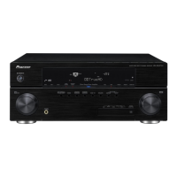
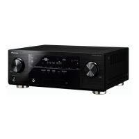
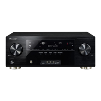
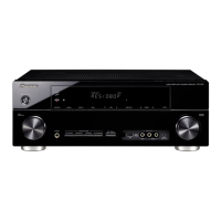
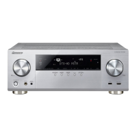
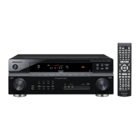
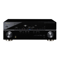
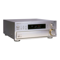
Explanation of front panel controls, indicators, and features.

8.2 SPECIFICATIONS

Detailed technical specifications for Amplifier, FM Tuner, AM Tuner, and Video sections.

Audio Components Connections

Audio Components Connections

Guide for connecting analog and digital audio components to the receiver.

Cassette deck placement

Advice on positioning cassette decks to avoid noise interference.

Related product manuals