EasyManua.ls Logo

Pioneer X-HM20-S Service Manual

Pioneer X-HM20-S
59 pages
To Next Page IconTo Next Page
Page #1 background imageLoading...
Page #1 background image
ORDER NO.
PIONEER CORPORATION 1-1, Shin-ogura, Saiwai-ku, Kawasaki-shi, Kanagawa 212-0031, Japan
PIONEER ELECTRONICS (USA) INC. P.O. Box 1760, Long Beach, CA 90801-1760, U.S.A.
PIONEER EUROPE NV Haven 1087, Keetberglaan 1, 9120 Melsele, Belgium
PIONEER ELECTRONICS ASIACENTRE PTE. LTD. 253 Alexandra Road, #04-01, Singapore 159936
PIONEER CORPORATION
2011
2011 Printed in Japan
X-HM20-K
RRV4220
CD Receiver System
X-HM20-K
X-HM20-S
X-HM10-K
X-HM10-S
THIS MANUAL IS APPLICABLE TO THE FOLLOWING MODEL(S) AND TYPE(S).
Model Type Power Requirement Serial No. Remarks
X-HM20-K SYXJC8 AC 220 V to 240 V &&&&######YY YY: Europe
X-HM20-S SYXJC8 AC 220 V to 240 V &&&&######YY YY: Europe
X-HM10-K SYXJC8 AC 220 V to 240 V &&&&######YY YY: Europe
X-HM10-S SYXJC8 AC 220 V to 240 V &&&&######YY YY: Europe
K-IZV SEPT.

Other manuals for Pioneer X-HM20-S

Question and Answer IconNeed help?

Do you have a question about the Pioneer X-HM20-S and is the answer not in the manual?

Pioneer X-HM20-S Specifications

General IconGeneral
DisplayLCD
Remote ControlYes
Frequency Response20Hz - 20kHz
InputsUSB, AUX
Playback MediaCD, USB
Supported Audio FormatsMP3
TunerFM Tuner
USBYes

Summary

SAFETY INFORMATION

WARNING

Product may contain chemicals known to cause cancer or birth defects.

LASER CHARACTERISTICS

Apparatus contains Class 1 Laser; servicing by instructed person.

SERVICE PRECAUTIONS

NOTES ON SOLDERING

Environmental protection, lead-free solder usage, and tip temperature guidelines.

SPECIFICATIONS

BLOCK DIAGRAM

OVERALL WIRING DIAGRAM

Shows the interconnections between major components and PCB assemblies.

OVERALL BLOCK DIAGRAM

Illustrates the system's functional blocks and their data flow.

DIAGNOSIS

TROUBLESHOOTING

Step-by-step troubleshooting guide for common issues like "No Power" and "NO DISC".

DISASSEMBLY

SCHEMATIC DIAGRAM

MAIN PCB ASSY (1/7)

Schematic diagram for the main PCB assembly, part 1 of 7.

MAIN PCB ASSY (2/7)

Schematic diagram for the main PCB assembly, part 2 of 7.

MAIN PCB ASSY (3/7)

Schematic diagram for the main PCB assembly, part 3 of 7.

MAIN PCB ASSY (4/7)

Schematic diagram for the main PCB assembly, part 4 of 7.
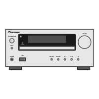
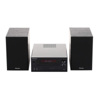
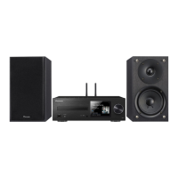
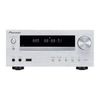
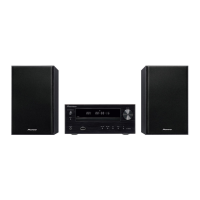
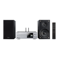
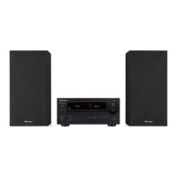
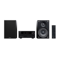
Related product manuals