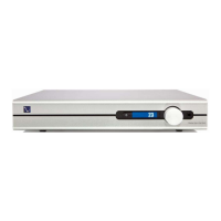
Owner’s Reference DirectStream Junior
4826 Sterling Drive, Boulder, CO 80301
PH: 720.406.8946 service@psaudio.com www.psaudio.com
©2016 PS Audio Inc. All rights reserved.
Introduction
®
3. The path from the single master clock to its retiming ip-op path is designed as short as
possible and isolated from all other clocking.
4. Connections between sections of the design have large impedances, not only lots of power
supply isolation, but also, for example, 2k resistors in series with digital signals to slow down the
edges and lessen any noise transfer.
5. Similarly we run I2C, SPI and other control signals as slowly as they can possibly go without
causing problems; we also control their transition times, thus limiting the amount of induced noise
and jitter into the main digital processing area.
6. Outputs of the FPGA use the slowest, lowest drive compatible with their function keeping noise
as low as possible.
7. We use slower, older technology CMOS when we need CMOS. This choice lowers both noise
and jitter potential.
8. We use balanced signals when practical, they not only lessen radiation and are less sensitive to
radiation, but they lessen noise in the ground and power rails.
9. We use non-saturation logic so the exact transitions are more predictable. Coming out of
saturation is a statistical process.
10. High rate signals (or signals with fast edges) are isolated from control signals and especially
each other. If they have to be fast they are terminated appropriately to help address jitter.
11. Jitter is addressed everywhere in the design. Every component choice, every signal connection,
every wire routed on the boards are all hand done to lower noise and pay attention to jitter.
12. 0.1% precision thin lm low temperature coecient resistors are incorporated everywhere in
the audio path. 2% lm caps in critical places and 5% lm caps elsewhere in the audio path. By
using 1/8W resistors or 1/4W resistors where others might use a 1/10W resistor the temperature
coecient of the resistors are lowered. For digital bypassing NP0/C0G or at worst X7R MLCCs
are used.
13. Low noise techniques are employed such as liberal use of low inductance capacitor bypassing
with a self resonance frequency at the main clock rate to keep noise from ever
getting into the voltage rails in the rst place.
14. Digital ltering in general, and the upsampling and noise shaping lters in the sigma-
delta modulators in particular, oer many degrees of freedom for a lter designer. There isn’t
a mathematically perfect lter to use (they all have tradeos), so we’ve chosen the lters that
sound best in our experience and in addition to that we run everything with as wide of an audio
bandwidth as possible.
15. Although design choices might have been made to run everything at single rate DSD (64 *
44100Hz), it was decided instead to run at double rate DSD to have a wider audio band below the
upsampling and noise shaping lters. Noise shaping is how a high rate sampled signal can have
Connection
impedances
Double DSD
Balanced
architecture
Signal isolation
Hand selected
parts