Tel : 886-2-29162151
Fax: 886-2-29174598
VFD Driver/Controller IC PT6315
PT6315 v2.0 Page 13 Sep. 2002
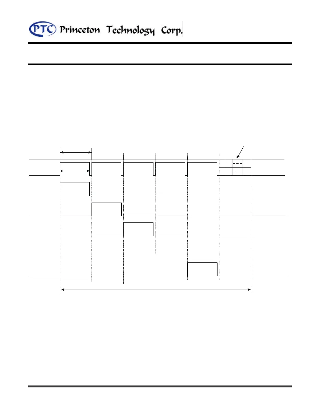
SCANNING AND DISPLAY TIMING
The Key Scanning and display timing diagram is given below. One cycle of key scanning consists of 2 frames.
The data of the 16 x 2 matrix is stored in the RAM.
Internal Operating Frequency (fosc) = 224/T
Figure 12: PT6315 Scanning & Display Timing Diagram
9 10 16
SGn
G1
G2
G3
DISPLAY
Gn
1 Frame=Tx (n +1)
DISPLAY
T
Note: T is the width of Segment only