LTE Standard Module Series
EC200U_Series_Hardware_Design 63 / 94
4.3. Reference Design of RF Layout
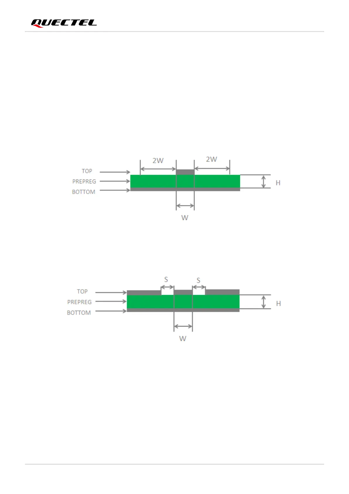
For user’s PCB, the characteristic impedance of all RF traces should be controlled as 50 Ω. The
impedance of the RF traces is usually determined by the trace width (W), the materials’ dielectric constant,
height from the reference ground to the signal layer (H), and the space between the RF trace and the
ground (S). Microstrip and coplanar waveguide are typically used in RF layout to control characteristic
impedance. The following figures are reference designs of microstrip or coplanar waveguide with different
PCB structures.
.
Figure 31: Microstrip Design on a 2-layer PCB
Figure 32: Coplanar Waveguide Design on a 2-layer PCB