1.0
EG21-G
PROJECT
TITLE
Lorry XU
Woody WU
CHECKED BY
DRAWN BY
OF
A
6
5
4
32
1
SHEET
A
B
C
D
123456
D
C
B
Quectel Wireless Solutions
SIZE
VER
145 DATE
2019/12/5
A2
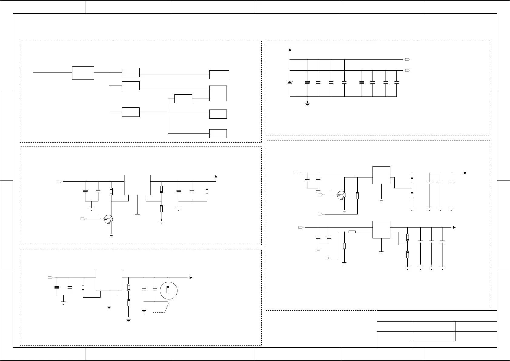
Reference Design
DC-DC Application
Notes:
2. VBAT should be routed in star mode to VBAT_BB and VBAT_RF pins.
Power Supply Design
VBAT Design
Closed to VBAT_BB pins.
Closed to VBAT_RF pins.
1. The power supply must be able to provide sufficient current up to 2A or more.
VDD_1V8 = (R0310/R0312+1)*1.207 = 1.8V
Power Supply for PCM Codec
VDD_3.3V = (R0305/R0308+1)*1.207 = 3.3V
LDO Application
It is used when the input voltage is below 7V.
VBAT = (R0301/R0307+1)*1.24 = 3.88V
The recommended load current is greater than 10mA.
Power Supply for SGMII and SD Card
VBAT = (R0314/R0318+1)*1.24 = 3.3V
Note:
DC-DC LDO
LDO
DC 1.8V
LDO
DC 3.3V
Codec
LDO
DC 3.3V 3.0A
EG21-G
SD Card
DC 5V OUT
DC 3.8V 2.0A
e.g. DC12V IN
3. The recommended operating voltage of VBAT is 3.3V~4.3V.
The recommended load current of MIC29302WU is greater than 10mA.
Notes:
1. CODEC_POWER_EN must be at low level in order to ensure the normal output voltage of VDD_3.3V.
2. The following power-on/off sequences should be complied with to ensure the audio codec
Power-on Sequence: power on VDD_1V8 first, then VDD_3.3V.
Note 1
If VDD_3.3V power supply needs to be switched off, please keep CODEC_POWER_EN at high level.
SGMII
It is used when the input voltage is above 7V. Use a DC-DC converter to convert a high input voltage
into a 5V output, and then the LDOs will generate 3.8V, 3.3V and 1.8V typical voltages.
Power-off Sequence: power off VDD_3.3V first, then VDD_1V8.
works normally.
+
C0301
100μF
C0302
100nF
C0303
33pF
C0304
10pF
C0306
100nF
C0307
33pF
C0308
10pF
+
C0305
100μF
D0301
WS4.5D3HV
1
IN
3
EN
5
OUT
4
BP
2
GND
U0303
SGM2019-ADJYN5G/TR
C0320
4.7μF
R0310
39K
1%
R0312
75K
1%
C0318
100nF
C0321
100nF
C0322
33pF
C0319
1μF
C0315
4.7μF
R0305
73.2K
1%
R0308
42.2K
1%
C0316
100nF
C0313
1μF
C0314
100nF
1
IN
3
EN
5
OUT
4
BP
2
GND
U0302
SGM2019-ADJYN5G/TR
C0317
33pF
R0306
10K
+
C0311
470μF
1
EN
2
IN
3
GND
4
OUT
5
ADJ
U0301
MIC29302WU
C0312
100nF
C0310
100nF
+
C0309
470μF
R0301
100K
1%
R0307
47K
1%
R0302
51K
R0303
330R
Q0301
DTC043ZEBTL
R0311
100K
R0309
0R
+
C0325
470μF
1
EN
2
IN
3
GND
4
OUT
5
ADJ
U0304
MIC29302WU
C0326
100nF
C0324
100nF
+
C0323
470μF
R0314
75K
1%
R0318
47K
1%
R0313
51K
R0315
330R
Q0304
DTC043ZE
[3,5,14]
VBAT
[3,5,14]
VBAT
VBAT
VDD_1V8
VDD_3.3V
[4,5,14]
DC_5V
[4]
CODEC_POWER_EN
[4,5,14]
DC_5V
VBAT
[4]
VBAT_EN
[4,5,14]
DC_5V
[3,4,6,11,13,14]
VDD_EXT
[4,5,14]
DC_5V
VDD3V3
[5,7,8]
VDD_1V8
 Loading...