1.0
EG21-G
PROJECT
TITLE
A2
Reference Design
2019/12/5
DATE814
VER
SIZE
Quectel Wireless Solutions
B
C
D
6543 21
D
C
B
A
SHEET
1
23
4
5
6
A
OF
DRAWN BY
CHECKED BY
Woody WU
Lorry XU
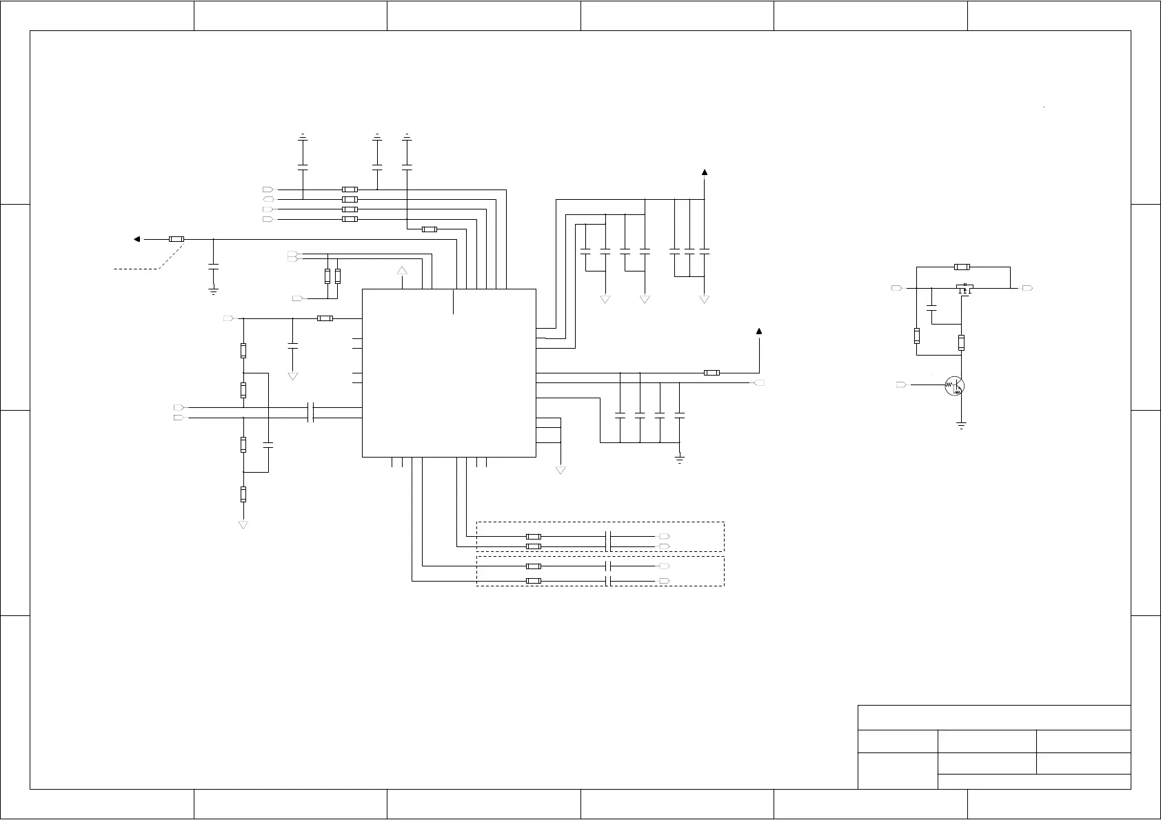
Power on reset
Differential signals, and are connected to handset and audio power amplifier.
Left and right channels, and are connected to headset.
Delay Circuit
Audio Codec Design (TLV320AIC3104)
1. TLV320AIC3104 power-on sequence: IOVDD -> AVDD/DRVDD -> DVDD -> software initialization.
Notes:
2. The RC delay circuit, which is assembled with C0621 and R0608, is used to ensure that the power-on time difference between AVDD and DVDD is within 5ms.
4. EG21-G will automatically initialize the codec via I2C interface after it is turned on successfully,
3. The RESET pin must be driven at low level for at least 10ns after all power supplies for TLV320AIC3104 are at their specified values.
5. The AGND and DGND of TLV320AIC3104 are connected together through 0R resisitor R0703 in Sheet 7.
so all power supplies for the codec need to be powered on before that.
6.The maximum output power of the codec is 15mW when the surround stereo headphone driver with 32Ω load is used, and is 30mW when the surround stereo
headphone driver with 16Ω load is used.
1
MCLK
2
BCLK
3
WCLK
4
DIN
5
DOUT
6
DVSS
7
IOVDD
8
SCL
9
SDA
10
MIC1LP/LINE1LP
11
MIC1LM/LINE1LM
12
MIC1RP/LINE1RP
13
MIC1RM/LINE1RM
14
MIC2L/LINE2L/MICDET
15
MICBIAS
16
MIC2R/LINE2R
17
AVSS1
18
DRVDD
19
HPLOUT
20
HPLCOM
21
DRVSS
22
HPRCOM
23
HPROUT
24
DRVDD
25
AVDD
26
AVSS2
27
LEFT_LOP
28
LEFT_LOM
29
RIGHT_LOP
30
RIGHT_LOM
31
RESET
32
DVDD
33
GND
U0601
TLV320AIC3104
C0619
100nF
C0618
100nF
R0614
1.5K
R0616
1.5K
C0613
2.2μF
C0605
100nF
C0611
10uF
C0606
1μF
C0607
100nF
C0608
1μF
C0610
1μF
C0614
100nF
C0615
1μF
R0613
0R
C0616
100nF
C0617
1μF
C0622
1μF
C0623
1μF
R0607
10K
R0605
0R
R0604
0R
R0601
0R
R0603
0R
C0612
100nF
C0603
NM
C0601
NM
C0602
NM
C0609
100nF
R0609
1K
R0612
1K
C0620
10μF
R0610
4.7K
R0611
4.7K
R0617
10K
G
SD
Q0601
Si2333DS-T1-E3
C0621
10nF
R0608
100K
Q0602
DTC043ZEBTL
R0615
NM_0R
C0624
22μF
C0604
22μF
R0606
NM_0R
R0602
0R
R0618
0R
R0619
0R
R0620
0R
R0621
0R
[7,9]
MIC_P
[7,9]
MIC_N
MICBIAS_3104
[3,7]
I2C_SCL
[3,7]
I2C_SDA
VDD_3.3V
VDD_1V8
[7,9]
SPK_P
[7,9]
SPK_N
DVDD
[3,7]
CODEC_PCM_CLK
[3,7]
CODEC_PCM_SYNC
[7,9]
SPK_R
[7,9]
SPK_L
[5,7,8]
VDD_1V8
[8]
DVDD
[5,7,8]
VDD_3.3V
[8]
DVDD
[5,7,8]
VDD_1V8
[3,7]
CODEC_PCM_OUT
[3,7]
CODEC_PCM_IN
 Loading...