Renesas VUI Reference Solution VOICE-RA6E1 Engineering Manual
VOICE-RA6E1 Engineering Manual Rev.1.0 Page
of 14
June 2022
8.5 LEDs
3 LED are included on the board and are connected to the MCU I/O. These are Red, Green, and Blue, and
can be used for any user defined functions.
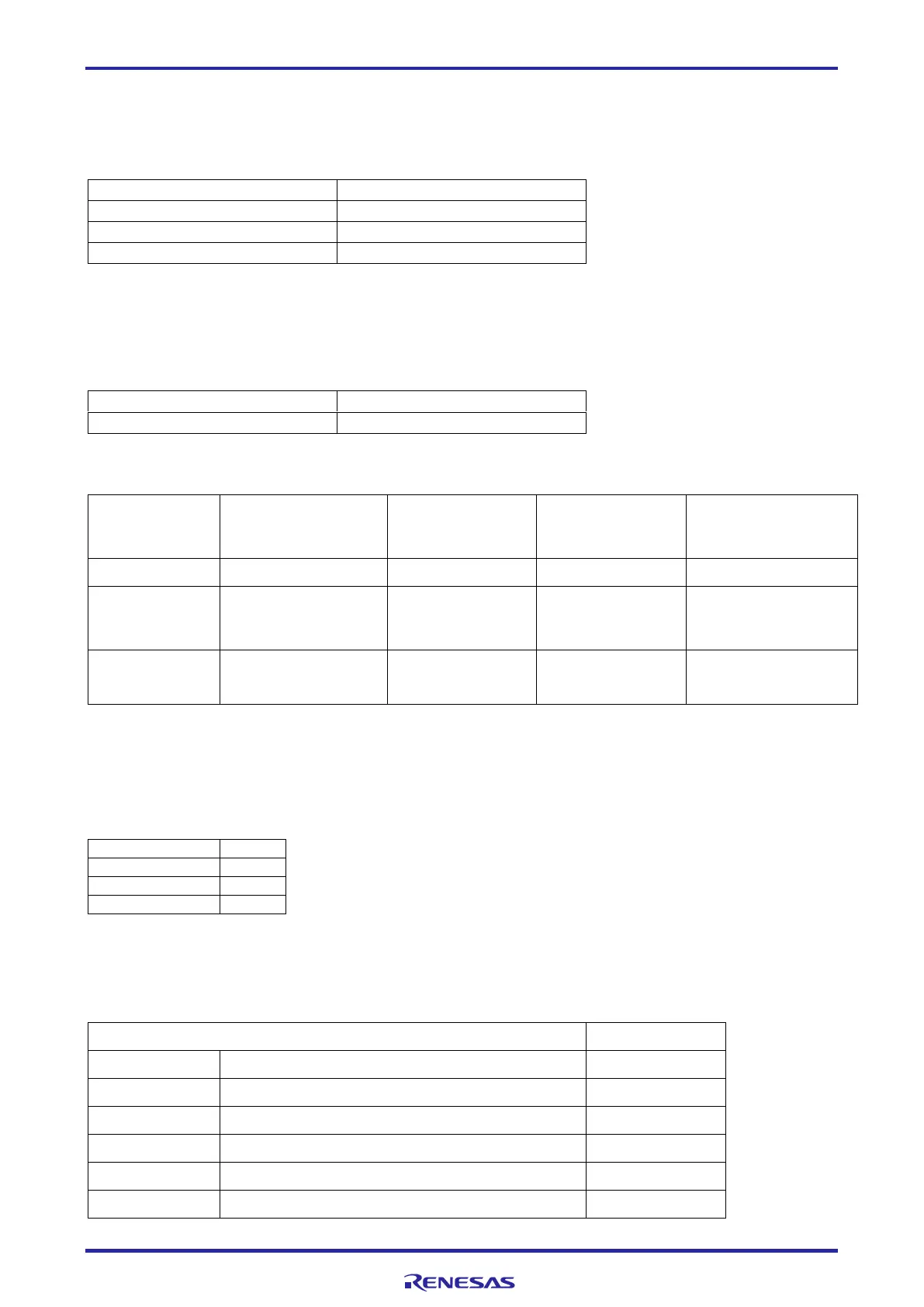
Table 11. User LED Port Assignments
D5 (blue) is power LED, and D8 (Green) is debug status LED to indicate the status of the JLOB connection.
8.6 Buttons
There are two mechanical push-button switches on the board. One button is for system/MCU reset (S2).
The second button is a user programmable button (S1).
Table 12. User Button Port Assignment (S1)
8.7 Debug
The VOICE-RA6E1 board supports following three debug modes.
Debug MCU
(one that connects
to the IDE on PC)
Target MCU
(one that is being
debugged)
Debugging
Interface/Protocol
20-pin connector (J9)
or 10-pin connector
(J8)
20-pin connector (J9)
or 10-pin connector
(J8)
Notes:
• Please cut E9 for Debug out function
• See Table 14 for the Debug USB connector pin definition.
• See Table 15 for the 10-pin JTAG connector pin definition.
• See Table 16 for the 20-pin JTAG connector pin definition.
Table 13. Jumper Connection Summary for Different Debug
The J-Link On-Board (JLOB) debug interface supporting JTAG, SWD debug interface and also supports the
VCOM (Virtual COM port) function. The debug MCU is a Renesas RA4M2, programmed with J-Link firmware
licensed by Segger. This interface includes one USB micro-B connector (J6) for host debug through the J-
Link MCU, one 10-pin and one 20-pin debug header (supporting JTAG and SWD).
Table 14. Debug USB Connector
USB ID, jack internal switch, cable inserted

 Loading...


