Renesas VUI Reference Solution VOICE-RA6E1 Engineering Manual
VOICE-RA6E1 Engineering Manual Rev.1.0 Page
of 14
June 2022
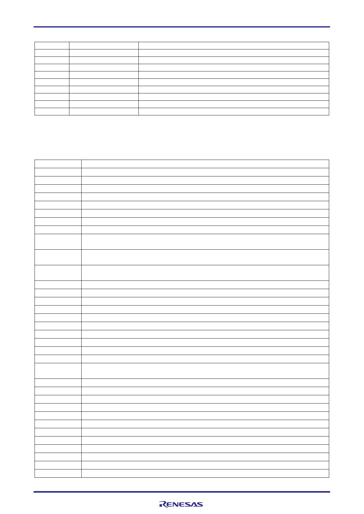
Table 2. Default Copper Jumper Settings
WS output to I2S digital microphone
SCK output to I2S digital microphone
MOSI for I2S digital microphone left channel
ADC0, Analog microphone left channel
ADC1, Analog microphone right channel
DA out to OPAMP, audio out
P201/MD signal, cut it then the J8, J9 can be debug out function
7. MCU Port Mapping
Here are the port and pin assignments for the kit.
Table 3. MCU Port Assignments
Analog microphone, left channel
Analog microphone, right channel
QSPI DQ1 for QSPI flash or MISO for I2S digital microphone right channel, mux by J12
jumper wire
QSPI DQ0 for QSPI flash or SCK for I2S digital microphone right channel, mux by J13
jumper wire
QSPI DQ3 for QSPI flash or WS for I2S digital microphone right channel, mux by J14
jumper wire
GPT1 output for SCK to I2S D-MIC
Debug, SWDIO for SWD or TMS for JTAG
MOSI for I2S digital microphone left channel, when debug, it is TDO for JTAG
LED3, user LED, blue color
Boot Mode, The MCU enter SCI and USB boot mode if the MD pin is held low on release
the reset signal, it is for download code to MCU flash memory.
WS for I2S digital microphone left channel
Clock Crystal, optional, not populated on this kit
Clock Crystal, optional, not populated on this kit
Debug, SWCLK for SWD or TCK for JTAG
WS for I2S digital microphone
LED2, user LED, green color

 Loading...


