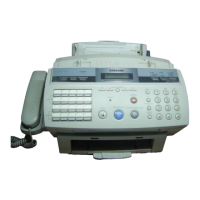
CIRCUIT DESCRIPTION
<1> General description
MAIN CONTROLLER(S3C46Q0X,U12) consists of this
system consists of CPU(ARM7TDMI RISC PROCES-
SOR), 8K BYTES CACHE, DATA and ADDRESS BUS,
PLL deriding input frequency and CLOCK CONTROL part,
SERIAL COMMUNICATION part supporting UART, PRINT
HEAD control part, PARALLEL PORT INTERFACE part,
USB INTERFACE part, Internal Image Processor Part,
External DMA part MEMORY and EXTERNAL BANK con-
trol part, SYNCHRONOUS SERIAL INTERFACE control
part for interfacing Quarter_Horse, and TX Motor drive con-
trol and general purpose I/O control parts.(See Figure 2 )
3.1.3.2 S3C46Q0X FUNCTION DESCRIPTION
<1> SYSTEM CLOCK
There are two ways of Clock input method. One is the
method to make Master Clock(MCLK) at the internal PLL
by connecting X-tal and Capacitor to the outside, and
another method is to use MCLK(When inputting 40MHz)
directly, which supplies maximum 40MHz Clock to the
EXTCLK terminal(PIN65). The range of frequency being
input in case of using X-tal is limited to 4MHz~10MHz.
For making the MCLK, the Clock is supplied to the
EXTCLK Terminal of the ASIC by sending output power
(32.256MHz) of the MODEM (FM214 or FM214-VS, U16)
XCLK via the RC Filter. The inner side of the ASIC takes
the Clock, and it goes to the MPLL circuit to create a basic
operating frequency (66MHz MCLK signal). Also the Clock
goes to the UPLL circuit to make the operating frequency
of the USB Controller (48MHz).
<2> DATA and ADDRESS BUS CONTROL
1. _RD & _WR
_RD & _WR SIGNAL are synchronized with the inside
MCLK(66MHZ) and becomes active to Low.
These signal are Strobe Signal used to Read or Write
data when each Chip Select becomes active connected
to SDRAM, ROM(Flash), _WR PIN, _RD of Modem.
2. CHIP SELECT
(_ROMCS, _IP_CS,_MED_CS,_SCS0,_SCS1)
• _ROMCS : FLASH MEMORY(U7) CHIP SELECT
(LOW ACTIVE)
• _MODEM_CS : MODEM(U16) CHIP SELECT
(LOW ACTIVE)
• _SCSO : SDRAM (BASIC 16MBIT(U9), TAD 64MBIT(U8),
CHIP SELECT (LOW ACTIVE)
In case each Chip Select is low, it may Read or Write data.
3. D0 ~ D15
• 16BIT DATA BUS
4. A0 ~ A24
• ADDRESS BUS (A23 ~ A24 RESERVED)
3.1.3.1 BLOCK DIAGRAM and MAIN CONTROLLER description
 Loading...