- 11 -
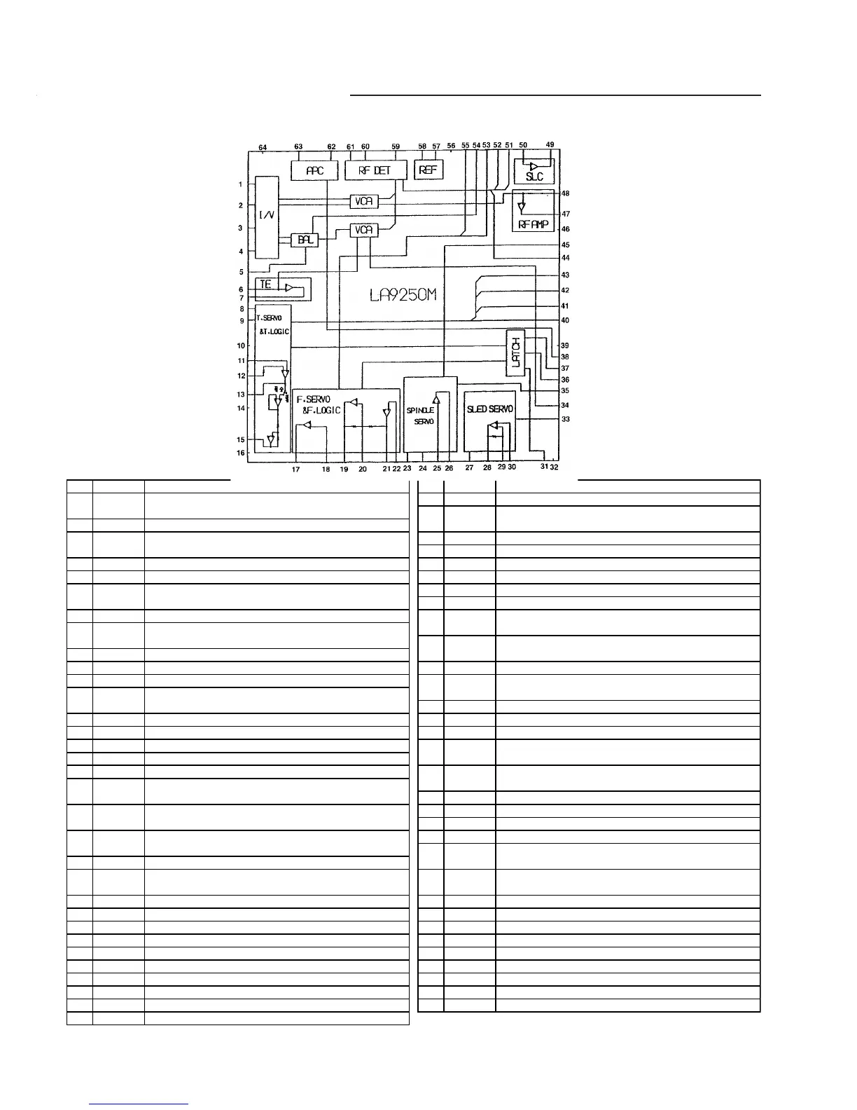
IC BLOCK DIAGRAM & DESCRIPTION
IC901 LA9250M (Analog Signal Processor)
No. Pin Name
Function
1 FTN2
Pick-up photo-diode connection pin. Added to FTN! Pin to generate the
RF signal, subtracted from FTN1 pin to generate the FE signal.
2 FTN1
Pick-up photo-diode connection pin.
3E
Pick-up photo-diode connection pin. Subtracted from F pin to generate
the TE signal.
4F
Pick-up photo-diode connection pin.
5TB
TE signal DC component input pin.
6 TE-
PIN which connect the TE signal gain setting resistor between this pin
and TE pin.
7TE
TE signal output pin.
8 TSEI
TES(Track Error Sense)comparator input pin. The TE signal is input
thorough a band-pass filter.
9 SCI
Shock detection input pin.
10 T H
Tracking gain time constant setting pin.
11 TA
TA amplifier output pin.
12 TD-
Pin for configuring the tracking phase compensation constant between
the TD and VR pin.
13 T D
Tracking phase compensation setting pin.
14 JP
Tracking jump signal(kick pulse)amplitude setting pin.
15 TO
Tracking control signal output pin.
16 N C
No connection
17 F D
Focusing control signal output pin.
18 FD-
Pin for configuring the focusing phase between the FD and FA pins.
19 FA
Pin for configuring the focusing phase compensation constant the FD-
and FA- pins.
20 FA-
Pin for configuring the focusing phase compensation constant between
the FAS and FE pins.
21 FE
FE signal output pin.
22 FE-
Pin which connects the FE signal setting resistor between this pin and
FE pin.
23 SP
Inverted output of CLV pin signal.
24 SPG
12-cm spindle mode gain setting resistor connection pin.
25 SP-
Spindle phase compensation constant pin, along with SPD pin.
26 SPD
Spindle control signal output pin.
27 SLEQ
Sled phase compensation constant connection pin.
28 SLD
Sled control signal output pin.
29 SL-
Input pin for sled movement signal from microprocessor.
30 SL+
Input pin for sled movement signal from microprocessor.
31 OSC
Pin for setting oscillating frequency.
32 N C
No connection.
No. PIN NAME Function
33 SLOF Sled servo off control input pin.
34 TGRF
Pin for setting the function on/off, which function is tracking gain
following to RF level.
35 SP8 Switch control pin for spindle 8cm/12cm mode.
36 EFBAL E/F balance control signal input.
37 FSTA Focus search control signal input.
38 LASER Laser on/off control input.
39 NC No connection.
40 TJP Input pin for tracking jump signal from DSP.
41 TGL
Input pin for tracking gain control signal from DSP. Gain is low when
TGL is high.
42 TOFF
Input pin for tracking off control signal from DSP. Tracking servo is off
when TOFF is high.
43 TES Output pin for TES signal to DSP.
44 HFL
The High Frequency Level is used to determine whether the main beam
is positioned over a pit or over the mirrored surface.
45 CLV Input pin for CLV error signal from DSP.
46 GND GND
47 RF RF output pin.
48 RF-
RF gain setting and EFM signal 3T compensation constant setting pin,
along with the RF pin.
49 SLC
Slice Level Control is an output pin that control the date slice level used
by the DSP for the RF wave-form.
50 SLI Input pin used by DSP for controlling the date slice level.
51 DEF Disc defect detection output pin.
52 DRF RF level detection output(Detect RF)
53 FSC Focus search smoothing capacitor output pin.
54 TBC
Tracking Balance Control; E/F balance adjustment variable range
setting pin.
55 FSS
Focus Search Select; focus search mode(+-search / + search vs. the
reference voltage) switching pin.
56 VCC VCC
57 REFI By-pass capacitor connection pin for reference voltage.
58 VR Reference voltage output pin.
59 LF2 Disc defect detection time constant setting pin.
60 PH1 RF signal peak hold capacitor connection pin.
61 BH1 RF signal bottom hold capacitor connection pin.
62 LDD APC circuit output pin.
63 LDS APC circuit input pin.
64 NC No connection.
 Loading...