- 63 -
IC BLOCK DAIGRAM & DESCRIPTION
IC500 M37903S4CHP (16-bit Micro Computer)
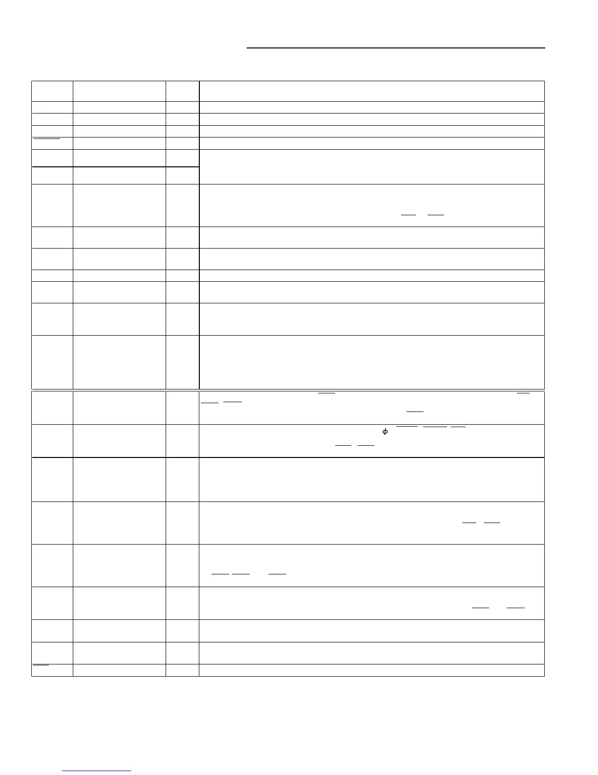
Pin Name
Input/
Output Description
V
CC
,V
SS
Power supply input Apply 5V ± 0.5V to Vcc, and 0V to Vss.
MD0 MD0 Input Connect this pin to Vcc.
MD1 MD1 Input Connect this pin to Vss.
RESET Reset input Input The microcomputer is reset when Vss-level voltage is applied to this pin.
X
IN
Clock input Input
X
OUT
Clock output Output
BYTE
External data bus width
select input
Input
This pin determines whether the external data bus has an 8-bit width or 16-bit width for the
memory expansion mode or microprocessor mode. The width is 16 bits when V
SS
-level
voltage is input, and 8 bits when V
CC
-level voltage is applied. When BYTE=V
SS
level, by the
resister setting, the external data bus for each of areas CS
1
to CS
3
can have a width of 8 bits.
CDSEL
Clock division select
input
Input
This pin determines the X
IN
-input-clock division select bit's (note) state at reset and the input
level at pin X
IN
.
AV
CC
,
AV
SS
Analog power supply
input
_
_
Power supply input pins for the A-D converter and the D-A converter. Connect AV
CC
to V
CC
,
and AV
SS
to V
SS
externally.
V
REF
Reference voltage input Input This is the reference voltage input pin for the A-D converter and the D-A converter.
P0
0
/A
16
-
P0
7
/A
23
Address (high-order)
output
Output
Address (A
16
-A
23
) is output. These pins also function as I/O port pins according to the resister
setting.
P1
0
/D
0
-
P1
7
/D
7
Data (low-order) I/O I/O
The low-order 8 bits of data (D
0
-D
7
) are input /output. When the external data bus has an 8-bit
width, address (LA
0
-LA
7
) output and data (D
0
-D
7
) input/output can be performed with the time-
sharing method, according to the resister setting.
P2
0
/D
8
-
P2
7
/D
15
I/O port p2,
Data (high-order) I/O
I/O
■ When 8-bit external data bus is used.
Port P2 is an 8-bit I/O port. This port has an I/O direction resister, and each pin can be
programmed for input or output. These pins enter the input mode at reset.
■ When 16-bit external data bus is used.
The high-order 8 bits of data (D
8
- D
15
) are input or output.
These are input and output pins of the internal clock generating circuit. Connect a ceramic or
quartz-crystal resonator between the X
IN
and X
OUT
pins. When an external clock is used., the
clock source should be connected to the X
IN
pin, and the X
OUT
pin s
P30 - P33 I/O port P3 I/O
P30 functions as an input pin of RDY; and P31, P32. P33 function as the output pins of RD,
BLW, BHW, respectively. P30 also functions as an I/O port pin according to the resister
setting. When the external data has a width of 8 bits, be BHW pin functions
P4
0 - P47 I/O port P4 I/O
P4
0
- P4
4
function as output or input pins of ALE, 1, HLDA, HOLD, CS
0
, and P4
5
- P4
7
as I/
port pins, respectively. According to the resister setting, P40 - P43 also function as I/O port
pins, and P4
5 - P47 as output pins of CS1 - CS3.
P5
0 - P57 I/O port P5 I/O
Port P5 is an 8-bit I/O port. This port has an I/O direction resister, and each pin can be
programmed for input or output. These pins enter the input mode at reset. These pins also
function as I/O pins for timers A0 - A3, output pins for the real-time output pins for the real-
time output, and input pins for the key-input interrupt.
P6
0 - P67 I/O port P6 I/O
Port P6 is an 8-bit I/O port. This port has an I/O direction resister, and each pin can be
programmed for input or output. These pins enter the input mode at reset. These pins also
function as I/O pins for timers A4, input pins for external interrupt inputs INT
0 - INT2, and input
pins for timers B0 - B2.
P7
0 - P77 I/O port P7 I/O
Port P7 is an 8-bit I/O port. This port has an I/O direction resister, and each pin can be
programmed for input or output. These pins enter the input mode at reset. These pins also
function as input pins for the A-D converter, output pins for the D-A converter, and input pins
for INT
2, INT3, and INT4.
P8
0 - P87 I/O port P8 I/O
Port P8 is an 8-bit I/O port. This port has an I/O direction resister, and each pin can be
programmed for input or output. These pins enter the input mode at reset.
These pins also function as I/O pins for UART0, UART1, and input pins for INT
3 and INT4.
P10
0/A0 -
P10
7A7
Address (low-order)
output
Output Address (A
0-A7) is output.
P11
0/A8 -
P11
7/A15
Address (middle-order)
output
Output
Address (A8-A15) is output. These pins also function as I/O port pins according to the resister
setting.
NMI Non-mask able interrupt Input This pin is for a non-mask able interrupt.
Note : The X
IN-input-clock division select bit is used to determine whether the input clock to pin XIN is to be divided or not.
 Loading...