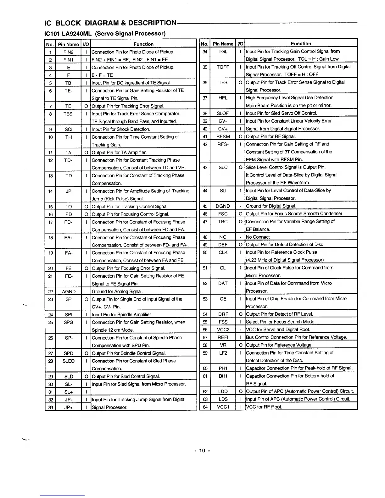
IC BLOCK DIAGRAM & DESCRIPTION
ICI 01 LA9240ML (Servo Signal Processor)
No.
34
35
36
37
39
33
40
41
42
43
44
45
46
47
46
49
50
51
52
53
54
55
56
57
56
.58
60
61
62
63
64
Jin Name
TGL
TOFF
TES
HFL
SLOF
cv-
Cv+
RFSM
RFS-
SLC
SLI
DGND
FSC
TBC
NC
DEF
CLK
CL
DAT
CE
DRF
FSS
VCC2
REFI
VR
LF2
PH1
BH1
LDD
LDS
Vccl
Uo
Function
I Input Pin for Tracking Gain Control Signal from
Digital Signal Processor. TGL = H : Gain Low
I Input Pin for Tracking Off Control Signal from Digital
Signal Processor. TOFF = H : OFF
o Output Pin for Track Error Sense Signal to Digital
Signal Processor.
I High Frequency Level Signal Use Detection
Main-Beam Position is on the pit or mirror.
I Input Pin for Sled Servo Off Control.
I Input Pin for Constant Linear Velocity Error
I
Signal from Digital Signal Processor.
o Output Pin for RF Signal.
I Connection Pin for Gain Setting of RF and
Constant Setting of 3T Compensation of the
EFM Signal with RFSM Pin.
o Slice Level Control Signal is Output Pin.
It Control Level of Data-Slice by Digital Signal
Processor of the RF Waveform.
I Input Pin for Level Control of Data-Slice by
Digital Signal Processor.
- Ground for D}gital Signal.
o Output Pin for Focus Search Smooth Condenser
o Connection Pin for Variable Range Setting of
EF Balance.
- No Connect
o Output Pin for Defect Detection of Disc.
I Input Pin for Reference Clock Pulse.
(4.23 MHz of Digital Signal Processor)
I Input Pin of Clock Pulse for Command from
Micro Processor.
I Input Pin of Data for Command from Micro
Processor.
I Input Pin of Chip Enable for Command from Micro
Processor.
o Output Pin for Detect of RF Level.
I Select Pin for Focus Search Mode
- VCC for Setvo and Digital Rcot.
I Bus Control Connection Pin for Reference Voltage.
o Output Pin for Reference Voltage.
I Connection Pin for Time Constant Setting of
Detect Detection of the Disc.
I Capacitor Connection Pin for Peak-hold of RF Signal.
I Capacitor Connection Pin for Bottom-hold of
RF Signal,
o Output Pin of APC (Automatic Power Control) Circuit.
I Input Pin of APC (Automatic Power Control) Circuit.
I VCC for RF Root.
-1o-
 Loading...