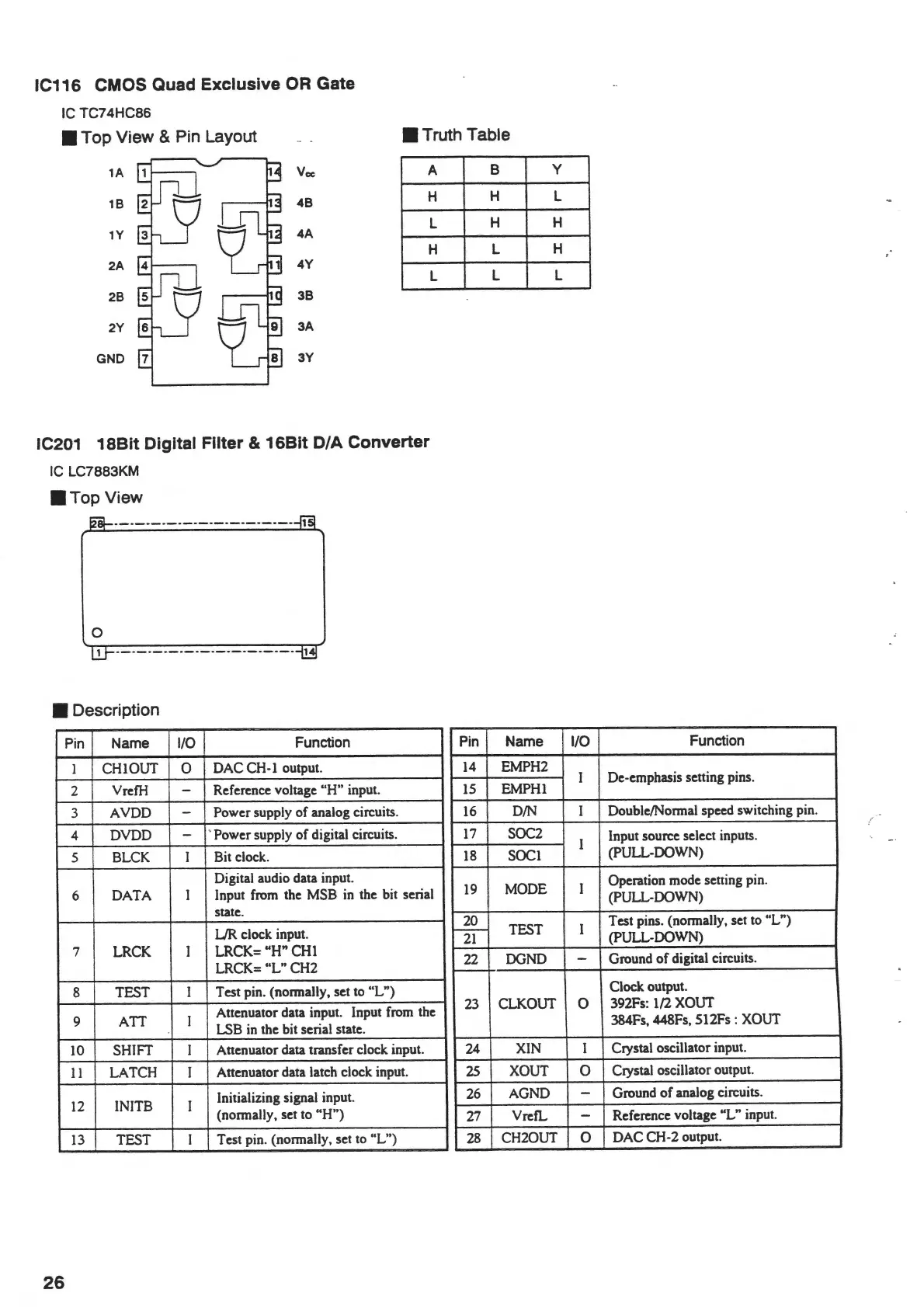
IC116 CMOS Quad
Exclusive
OR Gate
IC
TC74HC86
•Top
View & Pin Layout
•Truth
Table
1A A
18
48
H
1Y
4A
4Y
28
38
2Y
3A
3Y
IC201
18Bit
Digital
Filter
&
16Bit
DIA
Converter
IC
LC7883KM
•Top
View
·-·-·-·-·-·-·-·-·-·-·-·
1
0
1
·-·-·-·-·-·-·-·-·-·-·-·
1
• Description
Pin Name
1/0
Function
I CHI OUT
0
DAC CH-1 output.
2
VrefH
Reference voltage "H" input.
3 AVDD
Power supply
of
analog circuits.
4 DYDD
-
' Power supply
of
digital circuits.
5
BLCK Bit clock.
Digital audio data input.
L
H
L
6 DATA Input from the MSB in the bit serial
state.
UR
clock input.
7
LRCK
LRCK="H"CHl
LRCK=
"L"
CH2
8 TEST Test pin. (normally, set to "L")
9
ATT
Attenuator data input. Input from the
LSB in the bit serial state.
JO
SHIFT
Attenuator data transfer clock input.
11
LATCH
Attenuator data latch clock input.
12
INITB
Initializing signal input.
(normally, set to "H")
13
TEST Test pin. (normally, set to "L")
26
B
H
H
L
L
Pin
Name
14
EMPH2
15
EMPHl
16
DIN
17
SOC2
18
SOC!
19
MODE
20
TEST
-
21
22
DGND
23 CLKOUT
24 XIN
25
XOUT
26 AGND
27 VrcfL
28
CH20UT
y
L
H
H
L
1/0
Function
I
De-emphasis setting pins.
I
Double/Normal speed switching pin.
Input source select inputs.
I
(PULL-OOWN)
I
Operation mode setting pin.
(PULL-OOWN)
I
Test pins. (normally, set to "L")
(PULL-OOWN)
-
Ground
of
digital circuits.
Clock output.
0
392Fs: 1/2 XOUT
384Fs, 448Fs,
512Fs:
XOUT
I
Crystal oscillator input.
0
Crystal oscillator output.
-
Ground
of
analog circuits.
-
Reference voltage "L" input.
0
DAC CH-2 output.
 Loading...