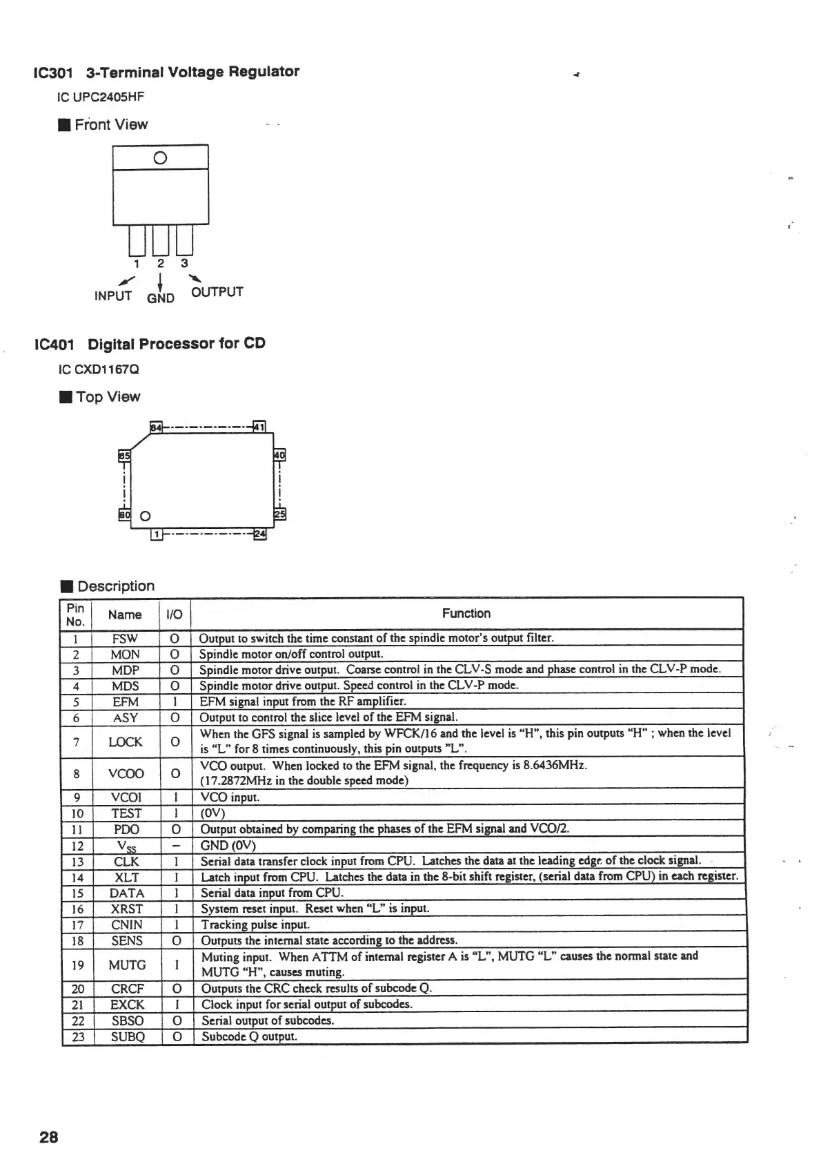
IC301 3-Terminal Voltage Regulator
IC UPC2405HF
•Front
View
0
2
•
1
/
INPUT
GND
"
OUTPUT
IC401 Digital Processor for CD
IC CXD1167Q
•TopView
1
·-·-·-·-·-·
•Description
Pin
j
No.
Name 1/0 Function
I
FSW
0
Output
to
switch the time constant
of
the spindle motor's output filter.
2
MON
0
Spindle motor on/off control output.
3
MOP
0
Spindle motor drive output. Coarse control
in
the CLV-S mode and phase control in the CLV-P mode.
4
MOS
0
Spindle motor drive output. Speed control
in
the CLV-P mode.
5
EFM 1 EFM signal input from the RF amplifier.
6 ASY
0
Output to control the slice level
of
the EFM signal.
7
LOCK
0
When the GFS signal
is
sampled
by
WFCK/16 and the level
is
"H", this pin outputs
"H";
when the level
is
"L" for 8 times continuously, this pin outputs "L".
8
vcoo
0
VCO output. When locked to the EFM signal, the frequency is 8.6436MHz.
(17.2872MHz in the double speed mode)
9
VCOI
I
VCO input.
10 TEST I
(OV)
II
PDO 0
Output obtained
by
comparing the phases
of
the EFM signal and VC0/2.
12
V~c::
-
GND(OV)
13
CLK I
Serial data transfer clock input from CPU. Latches the data at the leading
edgr:
of
the clock signal.
14
XLT I Latch input from CPU. Latches the data in the 8-bit shift register, (serial data from CPU) in each register.
15
DATA I Serial data input from CPU.
16
XRST 1
System reset input. Reset when "L" is input.
17
CNIN 1 Tracking pulse input.
18
SENS
0
Outputs the internal state according to the address.
19
MUTG I
Muting input. When A
TIM
of
internal register A
is
"L", MUTG "L" causes the normal state and
MUTG "H", causes muting.
20 CRCF
0
Outputs the CRC check results
of
subcode
Q.
21
EXCK I Clock input for serial output
of
subcodes.
22 SBSO
0
Serial output
of
subcodes.
23 SUBQ
0
Subcode Q output.
28
 Loading...