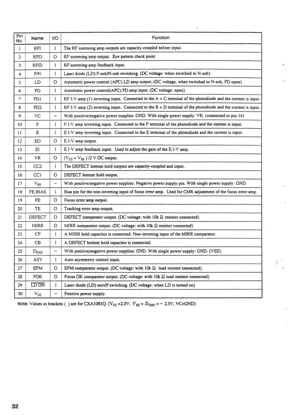
Pin
j
Name
I
1/0
Function
No. ,
I
I
RF!
I
The RF summing amp outputs arc capacity-coupled before input.
2
I
RFO 0
RF summing amp output. Eye pattern check point
3
RF8
I
RF summing amp feedback input.
4
PIN
I
Laser diode (LD) P-sub/N-sub switching. (DC voltage: when switched to N-sub)
5
LD
0
Automatic power control (APC) LD amp output. (DC voltage, when switched to N-sub, PD open)
6 PD
I
Automatic power control(APC) PD amp input. (DC voltage: open)
7
PDI I
RF
1-V
amp
(I)
inverting input.
Connected to the A + C terminal
of
the photodiode and the current
is
input.
8 PD2 I
RF
1-V
amp (2) inverting input.
Connected to the B + D terminal
of
the photodiode and the current
is
input.
9
vc -
With positive/negative power supplies: GND. With single power supply: VR. (connected to pin 14)
IO
F I
F 1-V amp inverting input. Connected to the F terminal
of
the photodiode and the current is input.
II
I
E
I
E
1-V
amp inverting input.
Connected to the E terminal
of
the photodiode and the current is input.
I2
EO
0
E
1-V
amp output.
13 El
I
E
1-V
amp feedback input. Used to adjust the gain
of
the E
1-Y
amp.
14
VR
0
(V cc +
VEE
) /2 V DC output.
15
CC2
I
The DEFECT bottom hold outputs arc capaciiy-coupled and input.
16
CCI
0
DEFECT bottom hold output.
17
VEE
- With positive/negative power supplies: Negative power supply pin. With single power supply: GND.
I8
FE
BIAS I
Bias pin for the non-inverting input
of
focus error amp. Used for CMR adjustment
of
the focus error amp.
I9
FE
0
Focus error amp output.
20
TE
0
Tracking error amp output.
2I
DEFECT
0
DEFECT comparator output. (DC voltage: with
IOk
Q resistor connected)
22
I
MIRR
0
MIRR comparator output. (DC voltage: with !Ok Q resistor connected)
23 I
CP
I
A MIRR hold capacitor
is
connected. Non-inverting input
of
the MIRR comparator.
24
I
CB I
A DEFECT bottom hold capacitor
is
connected.
25
Dcr>o
-
With positive/negative power supplies: GND. With single power supply: GND. (VEE)
26
ASY I
Auto asymmetry control input.
27 EFM
0
EFM comparator output. (DC voltage: with !Ok Q load resistor connected)
28 FOK
0
Focus OK comparator output. (DC voltage: with lOk Q load resistor connected)
29
LOON
I
Laser diode (LD) on/off switching. (DC voltage: when LD
is
turned on)
30
Yee
-
Positive power supply.
Note
: Values in brackets ( ) arc for
CXAI08IQ
. (V cc =2.SV,
VEE=
DcND
= - 2.SV, VC--GND)
32
 Loading...