High-Power Stereo Class-D Audio Power Amplifier
SGM4703 with Adjustable Power Limit and Automatic Level Control
5
DECEMBER 2022
SG Micro Corp
www.sg-micro.com
PIN DESCRIPTION (continued)
PIN NAME TYPE DESCRIPTION
14 MODS DI
PWM modulation select with an on-chip 250kΩ pull-up resistor to GVDD. A TTL logic input in
compliance with GVDD.
15, 16 PVDD P
Power supply inputs for the right-channel H-bridge. The power supplies for right-channel and
left-channel H-bridges are internally.
17 BSTPR AO
Connect to bootstrap holding capacitor for the right-channel non-inverting output, VOPR. A
0.1µF capacitor must be placed between this pin and VOPR for proper operation.
18 VOPR AO Right-channel non-inverting audio output terminal.
19 PGND G
Power ground for the right-channel H-bridge. Connect to the system ground GND. The power
ground for right-channel and left-channel H-bridges are internally shorted.
20 VONR AO Right-channel inverting audio output terminal.
21 BSTNR AO
Connect to a bootstrap holding capacitor for the right-channel inverting output, VONR. A
0.1µF capacitor must be placed between this pin and VONR for proper operation.
22 BSTNL AO
Connect to a bootstrap holding capacitor for the left-channel inverting output, VONL. A 0.1µF
capacitor must be placed between this pin and VONL for proper operation.
23 VONL AO Left-channel inverting audio output terminal.
24 PGND G
Power ground for the left-channel H-bridge. Connect to the system ground GND. The power
ground for right-channel and left-channel H-bridges are internally shorted.
25 VOPL AO Left-channel non-inverting audio output terminal.
26 BSTPL AO
Connect to a bootstrap holding capacitor for the left-channel non-
inverting output, VOPL. A
0.1µF capacitor must be placed between this pin and VOPL for proper operation.
27, 28 PVDD P
Power supply inputs for the left-channel H-bridge. The power supplies for right-channel and
left-channel H-bridges are internally shorted.
GND G Exposed pad. Connect to the system ground GND.
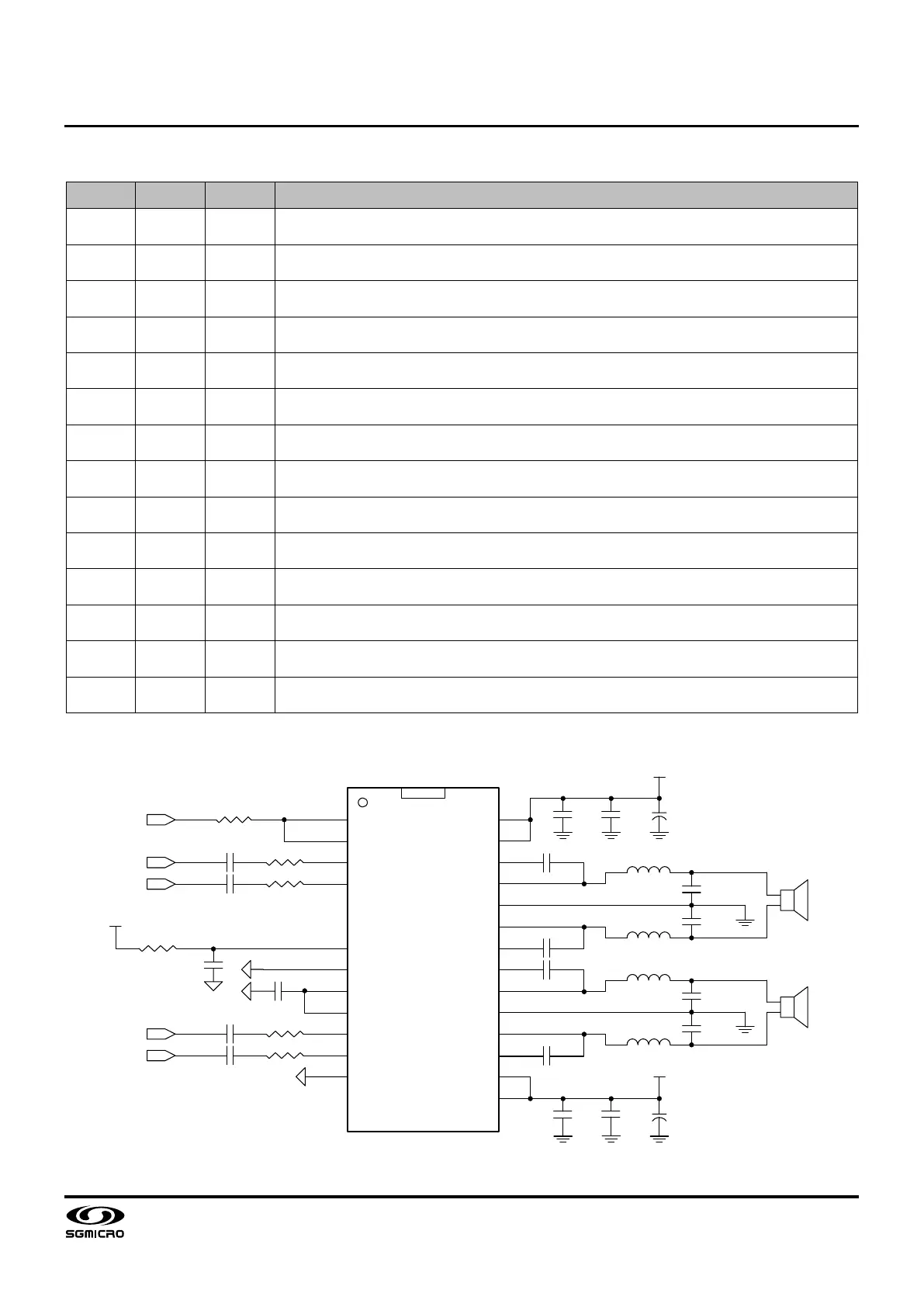
TYPICAL APPLICATION
SGM4703
EN
FAULTB
INPL
INNL
GAIN
FREQ
AV DD
AG ND
GV DD
PLIMIT
INNR
INPR
ALC
MODS
PV DD
PV DD
BS TPL
VO PL
PG ND
VO NL
BS TNL
BS TNR
VO NR
PG ND
VO PR
BS TPR
PV DD
PV DD
1
2
3
4
5
6
7
8
9
10
11
12
13
14
28
27
26
25
24
23
22
21
20
19
18
17
16
15
EN
INPL
INNL
V
DD
R
EN
10 kΩ
INNR
INPR
C
AV D D
1μF
C
G V DD
1μF
LS L
LS R
SP EAK ER
SP EAK ER
C
B
0. 1μF
C
B
0. 1μF
C
B
0. 1μF
C
B
0. 1μF
V
DD
C
PV D D
10 nF
C
PV D D
1μF
C
PV D D
22 0μF
+
V
DD
C
PV D D
10 nF
C
PV D D
1μF
C
PV D D
22 0μF
+
R
AV D D
10Ω
C
IN
1μF
C
IN
1μF
C
IN
1μF
C
IN
1μF
R
IN E
0Ω
R
IN E
0Ω
R
IN E
0Ω
R
IN E
0Ω
Figure 1. Typical Application Circuit