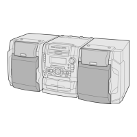
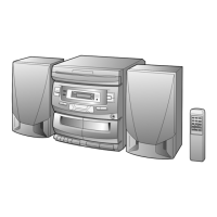
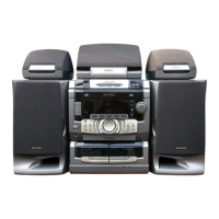
CD-C1W,CP-C1W
– 47 –
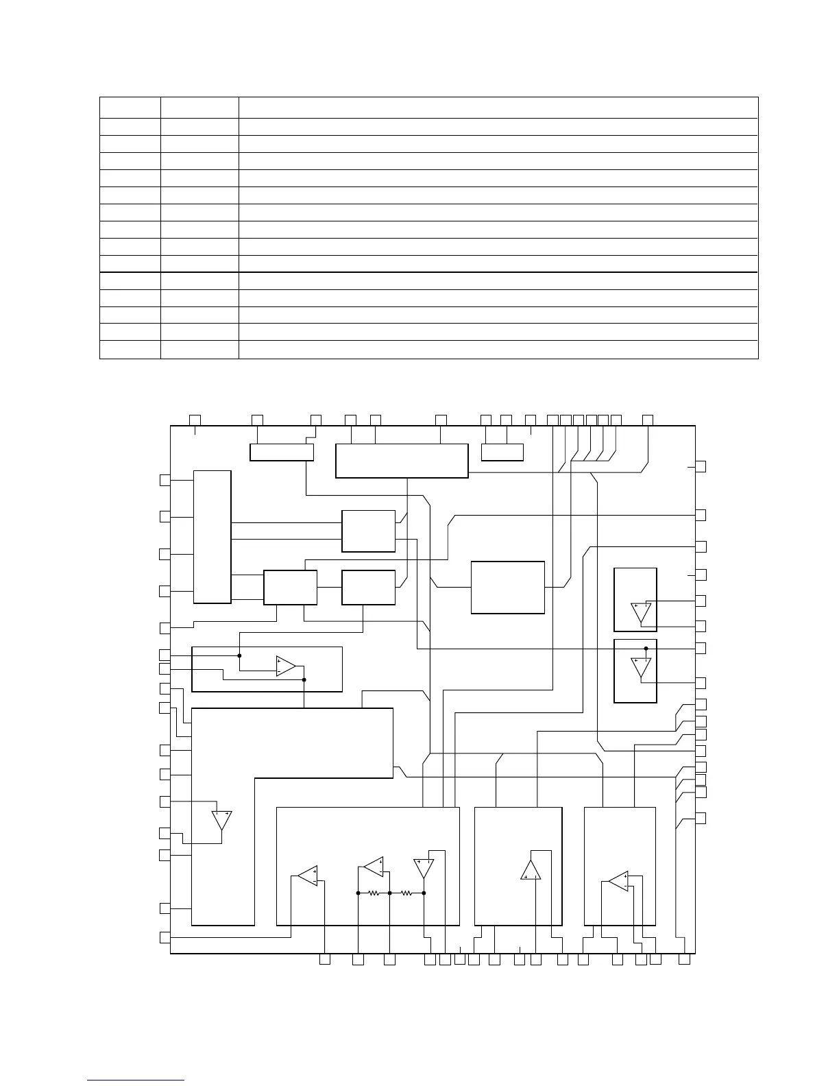
IC1 VHiLA9241M/-1:Servo Amp., (LA9241M) (2/2)
Pin No.
Port Name
Function
51 CL Micro computer command clock input pin.
52 DAT Micro computer command data input pin.
53 CE Micro computer command chip enable input pin.
54 DRF (DETECT RF) RF level detection output.
55 FSS (Focus Serch Select) Pin to switch focus search mode. (± search/+ search for reference voltage)
56 VCC2 VCC pin for servo system and digital system.
57 REFI Pin to connect pass control for reference voltage.
58 VR Reference voltage output pin.
59 LF2 Pin to set defect detection time constant of disk.
60 PHI Pin to connect capacitor for peak hold of RF signal.
61 BHI Pin to connect capacitor for bottom hold of RF signal.
62 LDD APC circuit output pin.
63 LDS APC circuit output pin.
64 VCC1 RF system VCC pin.
Figure 47 BLOCK DIAGRAM OF IC
IC1 VHiLA9241M/-1:Servo Amp., (LA9241M) (2/2)
1
FIN2
FIN1
E
F
TB
TE-
TE
TESI
SCI
TH
TA
TD-
TD
JP
TO
FD
FD-
FA
FE
JP+
TGL
TOFF
TES
HFL
SLOF
CV-
CV+
RFSM
RFS-
SLC
SLI
DGND
FSC
TBC
NC
DEFCLK
CL
DAT
CE
DRF
FSS
VCC2
REFI
VRLF2
PHI
BHI
LDDLDS
SLC
RF AMP
TE
F.SERVO & F.LOGIC SPINDLE SERVO SLED SERVO
VCC1
2
3
4
6
7
5
8
9
10
11
12
13
14
15
16
17
18
19
20
21 23
22
25
26
27 28
29
30
31
32
33
34
35
36
37
38
39
40
41
42
43
44
46
47
48
49
50
51
52
53
54
55
5657
58
59
61 60
62
63
64
45
24
APC
RF DET
REF
VCA
VCA
INTER FACE
BAL
µ-COM
I/V
T.SERVO & T.LOGIC
JP-
SL+
SL-SLDSLEO
SPO
SP-SPGSPISP
AGND
FE-FA-