– 47 –
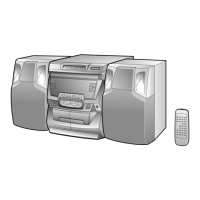
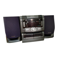
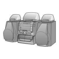
CD-C440W/CP-C440W
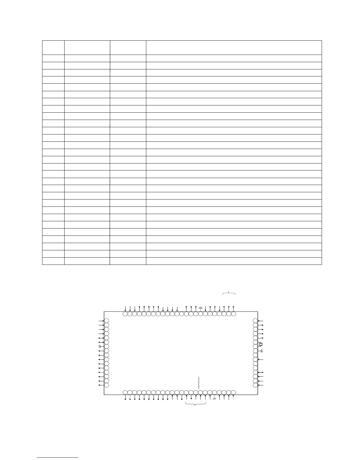
IC601 RH-iX0171AWZZ:System Microcomputer (IX0171AW) (2/2)
52 VDD — Positive power supply
53 CD O/C SW Input CD open-close switch input
54 DISC No. SW Input CD turntable position detection input
55 CD U/D SW Input CD mechanism UP/DOWN chucking detection input
56 T1 CrO SW Input Tape 1 CrO2 detection SW input
57 SRS INH Output SRS (surround) position selection output
58 SRS B Output SRS (surround) position selection output
59 SRS A Output SRS (surround) position selection output
60 SRS 3D Output SRS (surround) position selection output
61 SRS PASS Output SRS (surround) position selection output
62 SPAN 9K/10K Input Tuner span selector 9 kHz/10 kHz selection input
63 DOLBY Input DOLBY detection input, not applied in this machine
64 SRS Input SRS detection input, not applied in this machine
65 BALANCE Input BALANCE detection input, not applied in this machine
66 4SP Input 4SP detection input, not applied in this machine
67 TAPE A-FP SW Input Tape A side miserase preventing SW input
68 TAPE B-FP SW Input Tape B side miserase preventing SW input
69 TAPE PB MUT Output Tape playback mute output
70 TAPE T1/T2 Output Tape 1/2 selection
71 VLOAD — To be connected to GND
72 TAPE BIAS Output Tape bias circuit selection
73* ———— — Not used
74* ———— — Not used
75 TAPE BEET CUT Output Beat cancel signal control output
76 TAPE HI SPEED Output Tape mechanism High-Low speed selection
77* ———— — Not used
78* ———— — Not used
79* TAPE PB EQ Output Tape circuit playback Eq selection
80 TAPE REC MUT Output Tape circuit record muting output
In this unit, the terminal with asterisk mark (*) is (open) terminal which is not connected to the outside.
Terminal Name
Pin No. Input/Output
Function