– 59 –
CD-DK2600V
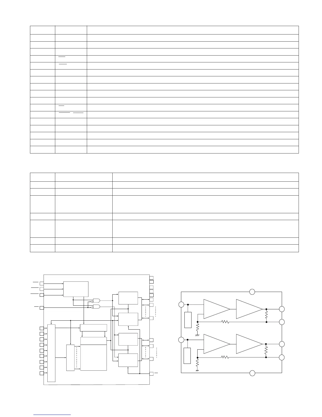
Pin No.
Port Name
Function
1 VCC Power supply
2-10 I/O0-I/O7 Data input/output
11*,12* NC Not used
13 WE Read/write enable
14 RAS Row address strobe
15* NC Not used
16-19 A0-A3 Address input (row/refresh: A0 to A3) (Column: A0 to A3)
20 VCC Power supply
21 VSS Ground
22-26 A4-A8 Address input (row/refresh: A4 to A8) (Column: A4 to A8)
27 OE Output enable
28,29 UCAS, LCAS Column address strobe
30* NC Not used
31-34 I/O8-I/O11 Data input/output
35 VSS Ground
36-39 I/O12-I/O15 Data input/output
40 VSS Ground
ICV3 VHiSDM4260C-1: DRAM (SDM4260C)
In this unit, the terminal with asterisk mark (*) is (open) terminal which is not connected to the outside.
RAS
LCAS
UCAS
WE
A0
A1
A2
A3
A4
A5
A6
A7
A8
VCC
VSS
I/O0
I/O1
I/O7
I/O8
I/O9
I/O15
OE
Lowar
Upper
Clock generating
circuit
Lower data
Input buffer
Lower data
Output buffer
Coidmn decoder
Upper data
Input buffer
A0-A8
A0-A8
I/O control circuit
Memory cell array
Upper data
Output buffer
Roe decoder
Row and column address buffer
14
29
28
13
16
17
18
19
22
23
24
25
26
27
39
32
31
10
3
2
40
35
21
1
20
Pin No.
Terminal Name
Function
1 Clamp input terminal Input of 1.9 V clamp, 1 Vp-p composite or Y-signal
2 GND Ground
3 Sag correction terminal Able to obtain an output without any sag by feeding back the sag, generated from output
coupling C, using the external C (see block diagram).
When not using the sag correction terminal, connect directly to the pin 4.
4,5 Output terminal 6 dB amplifier output. Able to drive 75? line.
6 Sag correction terminal Able to obtain an output without any sag by feeding back the sag, generated from output
coupling C, using the external C (see block diagram).
When not using the sag correction terminal, connect directly to the pin 5.
7 V+ Power source
8 Clamp input terminal Input of 1.9 V clamp, 1 Vp-p composite or Y-signal.
ICV4 VHiNJM2267M-1: Video operation amp. (NJM2267M)
6dB
Amp
6dB
Amp
75Ω
Driver
75Ω
Driver
Vout2
75Ω
2.2Ω
2.0kΩ
Vout1
75Ω
V5AG2
V5AG1
GND
2.2kΩ
2.0kΩ
Clamp
Clamp
7
5
6
4
3
2
1
8
VIN2
VOUT2
(6dB)
VOUT2
VOUT1
(6dB)
VOUT1
V+
VIN1
Correction terminal
Correction terminal
Figure 59 BLOCK DIAGRAM OF IC
ICV3 VHiSDM4260C-1: DRAM (SDM4260C)
ICV4 VHiNJM2267M-1: Video operation amp.
(NJM2267M)