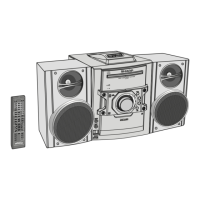
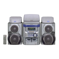
CD-DK890N
8 – 7
IC851 VHIAN80T53/-1: Multi Regulator (AN80T53)
Pin No. Terminal Name Function
1 REG4 Output 5.1 V power supply with a minimum peak out current of 1200 mA.
2 REG3 Output 13 V power supply with a minimum peak out current of 1350 mA.
3 VCC Connected to Power supplies.
4 GND Connected to the IC substrate.
5 MODE 1 REG1, REG2,REG3 and REG4 outputs are turned ON when this pin is 5 V.
6 REG2 Output 10 V power supply with a minimum peak out current of 800 mA.
7 REG1 Output 8.5 V power supply with a minimum peak out current of 700 mA.
5
2
3 4 1 7 6
Peak Current Protection,
Thermal Protection,
Load Short Protection.
Outputs
-
+
-
+
-
+
-
+
Prc
Drive
Reference
Voltage
MODE 1 REG 3 VCC GND
13V
REG4
5.1V
REG1
8.5V
REG2
10.0V
Prc
Drive
Prc
Drive
Prc
Drive
Figure 8-4: BLOCK DIAGRAM OF IC