LC-19LE320, LC-22LE320, LC-26LE320, LC-32LE320, LC-37LE320, LC-42LE320
132
• 1.8V ± 0.1V Power Supply Voltage
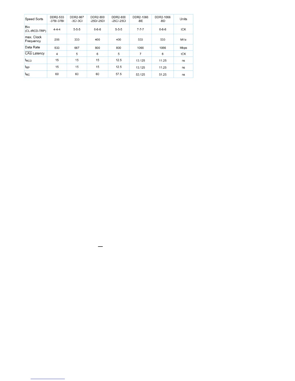
• Programmable CAS Latency: 3,4,5,6 and 7
• Programmable Additive Latency: 0, 1, 2, 3, and 4
• Write Latency = Read Latency -1
• Programmable Burst Length: 4 and 8
• Programmable Sequential / Interleave Burst
• OCD (Off-Chip Driver Impedance Adjustment)
• ODT (On-Die Termination)
• 4 bit prefetch architecture
• 1k page size for x 4 & x 8
2k page size for x16
• Data-Strobes: Bidirectional, Differential
• 4 internal memory banks
• Strong and Weak Strength Data-Output Driver
• Auto-Refresh and Self-Refresh
• Power Saving Power-Down modes
• Industrial grade device supports -40oC ~95oC operating
temperature. (-37BI/-3CI/-25DI/-25CI)
• 7.8 µs max. Average Periodic Refresh Interval
• Packages:
60 Ball BGA for x4/x8 components
84 Ball BGA for x16 component
• RoHS Compliance
Description
The 512Mb Double-Data-Rate-2 (DDR2) DRAMs is a highspeed CMOS Double Data Rate 2 SDRAM containing 536,870,912 bits. It is internally
configured as a quad-bank DRAM.
The 512Mb chip is organized as either 32Mbit x 4 I/O x 4 banks, 16Mbit x 8 I/O x 4 banks or 8Mbit x 16 I/O x 4 banks device.
The chip is designed to comply with all key DDR2 DRAM key features: (1) posted CAS with additive latency, (2) write latency = read latency -1, (3) normal
and weak strength dataoutput driver, (4) variable data-output impedance adjustment and (5) an ODT (On-Die Termination) function.
All of the control and address inputs are synchronized with a pair of externally supplied differential clocks. Inputs are latched at the cross point of
differential clocks (CK rising and CK falling). All I/Os are synchronized with a single ended DQS or differential DQS pair in a source synchronous fashion.
A 14 bit address bus for x4 and x8 organized components and a 13 bit address bus for x16 components is used to convey row, column, and bank address
devices.
These devices operate with a single 1.8V+/-0.1V power supply and are available in BGA packages.
An Auto-Refresh and Self-Refresh mode is provided along with various power-saving power-down modes.
1.4. U601 (TPA3110D2 15W TSSOP-28)
Features
· 15-W/ch into an 8- Load at 10% THD+N From a 16-V Supply
· 10-W/ch into an 8- Load at 10% THD+N From a 13-V Supply
· Operates from 8 V to 26 V
· 87% Efficient Class-D Operation Eliminates Need for Heat Sinks
· Four Selectable, Fixed Gain Settings
· Differential Inputs
· Thermal and Short-Circuit Protection With Auto Recovery Feature
· Speaker Protection Using Adjustable Power Limit
· DC Detect
· Surface Mount 28-pin TSSOP (PWP) Package
APPLICATIONS