LC32D44E/S/RU-BK/GY (1st Eddition)
5 – 21
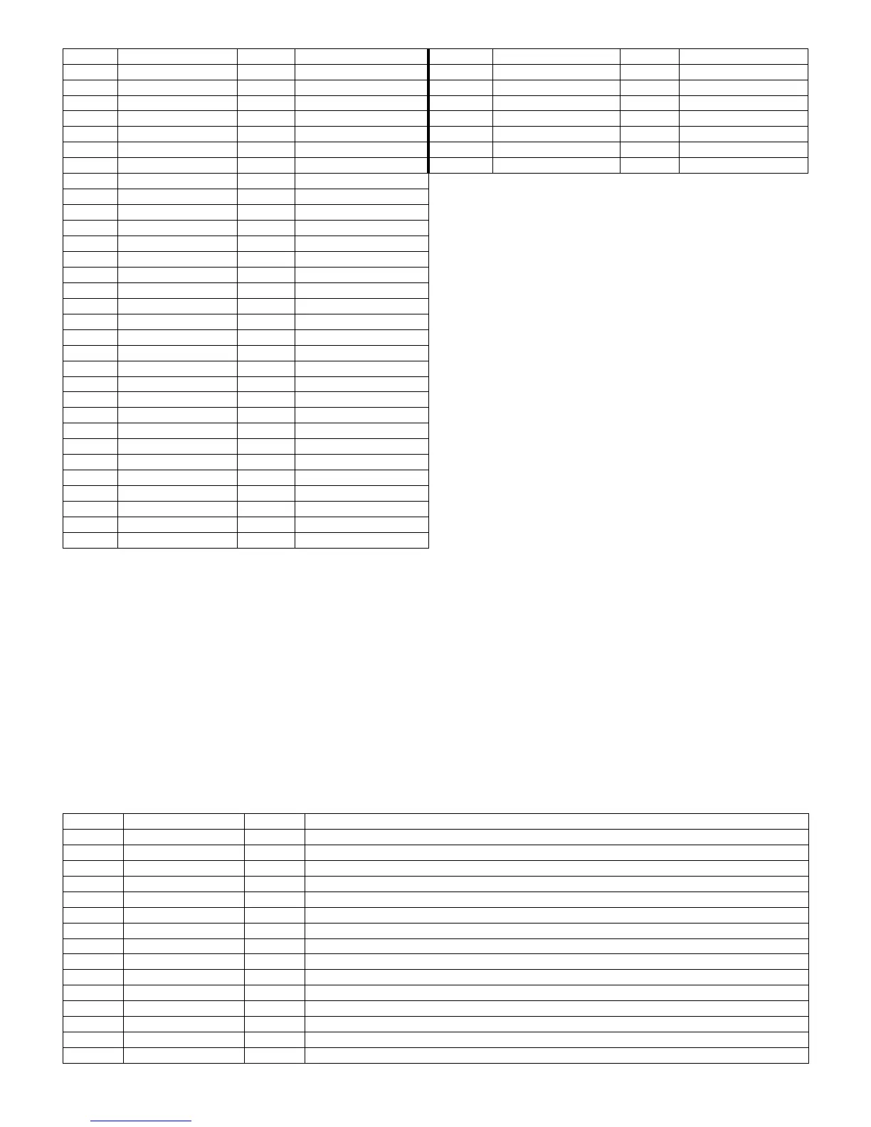
15. IC8201 (VHIBD8143MU-1Y)
High-accuracy gradation voltage generation IC with a built-in DAC
The high-accuracy gradation voltage generation IC with a built-in DAC, BD8143MUV, has a built-in 1chip integrating the setting value control by the
serial signal, high-accuracy 10bit DAC and buffer amp.
Description:
• Reduced number of parts due to 1chip
• Built-in 10bit DAC
• DAC output buffer amp (12ch)
• Amplifier input/output switching function (CTL)
• 3-wire serial interface
• Temperature protection circuit
• Power ON reset circuit
110 EX_DT[27] I/O BD4CIF 250 R_VSSPLL1 GND Z7RSTDDRVGND
111 EX_DT[28] I/O BD4CIF 251 R_VSSPLL2 GND Z7RSTDDRVGND
112 VDDC 1.5V VDDC 252 R_VDD15 1.5V Z7RSTDDRV15
113 VSS12 GND VSS12 253 R_VSS15 GND Z7RSTDDRVGND
114 EX_DT[29] I/O BD4CIF 254 VSSAGND45C GND Z7RSTAGND45C
115 vext158 1.5V SDRAMVDE1 255 VDDSAVCC5 3.3V Z7RSTAVCC5
116 VDDS 3.3V VDDS 256 VSSAGND45R GND Z7RSTAGND45R
117 VSS12 GND VSS12
118 vgnd50 GND SDRAMVSE
119 vext26 2.5V SDRAMVDE2
120 vgnd84 GND SDRAMVSE
121 EX_DT[30] I/O BD4CIF
122 EX_DIR I/O BD4CIF
123 TEST_C IN IBUFDIF
124 TEST_L[3] IN IBUFDIF
125 TEST_L[2] IN IBUFDIF
126 TEST_L[1] IN IBUFDIF
127 vgnd85 GND SDRAMVSE
128 vext1102 1.5V SDRAMVDE1
129 TEST_L[0] IN IBUFDIF
130 DAC_DATA OUT B4IF
131 DAC_CLK OUT B4IF
132 DAC_LATCH OUT B4IF
133 READY OUT B4IF
134 S_LBR OUT B4IF
135 G_LBR OUT B4IF
136 VDDS 3.3V VDDS
137 VSS12 GND VSS12
138 G_LBR_INV OUT B4IF
139 FS OUT B4IF
140 SREADY I/O BD4THVIC1
*Pin No.177, 178 is a power supply for SSCG, Pin No.180, 181 is GND for SSCG, and it is separated with another power supply GND.
Pin No. Pin Name I/O Pin Function
1 LATCH I Series latch input.
2 SDIN I Series data input
3 CLK I Series clock input
4 SDOUT O Series data output
5 DVCC --- Logic power supply
6 CT --- Capacity connection terminal for power ON reset.
7 GND --- Ground.
8 N.C --- No Connect.
9 OSC O DAC tune clock I/O.
10 N.C --- No Connect.
11 CTL I Amplifier input switch signal input.
12 N.C --- No connection.
13 VCC --- Buffer amplifier power supply.
14 OUT0 O Gradation voltage output terminal 0.
15 OUT1 O Gradation voltage output terminal 1.
Pin No. Pin Name I/O Function Name Pin No. Pin Name I/O Function Name