LC-37D90U
5 – 47
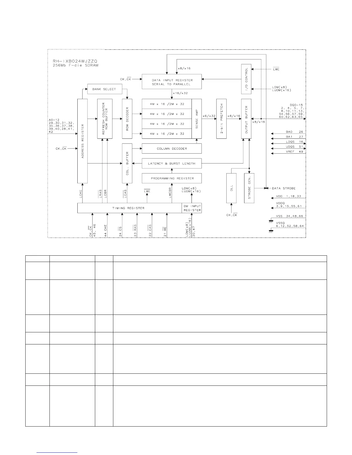
2.12. RH-iXB024WJZZQ (ASSY: IC8301-4)
256Mb F-die DDR SDRAM
• Block Diagram [RH-iXB024WJZZQ (ASSY: IC8301-4)]
• Pin Function [RH-iXB024WJZZQ (ASSY: IC8301-4)]
Pin No. Pin Name I/O Pin Function
45, 46 CK, CK I Clock : CK and CK are differential clock inputs. All address and control input signals are sampled on the
positive edge of CK and negative edge of CK. Output (read) data is referenced to both edges of CK.
Internal clock signals are derived from CK/CK.
44 CKE I Clock Enable : CKE HIGH activates, and CKE LOW deactivates internal clock signals, and device input
buffers and output drivers. Deactivating the clock provides PRECHARGE POWER-DOWN and SELF
REFRESH operation (all banks idle), or ACTIVE POWER-DOWN (row ACTIVE in any bank). CKE is
synchronous for all functions except for disabling outputs, which is achieved asynchronously. Input buff-
ers, excluding CK, CK and CKE are disabled during power-down and self refresh modes, providing low
standby power. CKE will recognize an LVCMOS LOW level prior to VREF being stable on power-up.
24 CS I Chip Select : CS enables (registered LOW) and disables(registered HIGH) the command decoder. All
commands are masked when CS is registered HIGH. CS provides for external bank selection on sys-
tems with multiple banks. CS is considered part of the command code.
23, 22,
21
RAS, CAS, WE I Command Inputs : RAS, CAS and WE (along with CS) define the command being entered.
20, 47 L(U)DM I Input Data Mask : DM is an input mask signal for write data. Input data is masked when DM is sampled
HIGH along with that input data during a WRITE access. DM is sampled on both edges of DQS.
Although DM pins are input only, the DM loading matches the DQ and DQS loading. LDM corresponds
to the data on DQ0~D7 ; UDM corresponds to the data on DQ8~DQ15. DM may be driven high, low, or
floating during READs.
26, 27 BA0, BA1 I Bank Addres Inputs : BA0 and BA1 define to which bank an ACTIVE, READ, WRITE or PRECHARGE
command is being applied.
29, 30,
31, 32,
35, 36,
37, 38,
39, 40,
28, 41,
42
A [0 : 12] I Address Inputs : Provide the row address for ACTIVE commands, and the column address and AUTO
PRECHARGE bit for READ/WRITE commands, to select one location out of the memory array in the
respective bank. A10 is sampled during a PRECHARGE command to determine whether the PRE-
CHARGE applies to one bank (A10 LOW) or all banks (A10 HIGH). If only one bank is to be pre-
charged, the bank is selected by BA0, BA1. The address inputs also provide the op-code during a
MODE REGISTER SET command. BA0 and BA1 define which mode register is loaded during the
MODE REGISTER SET command (MRS or EMRS).