LC-37D90U
5 – 49
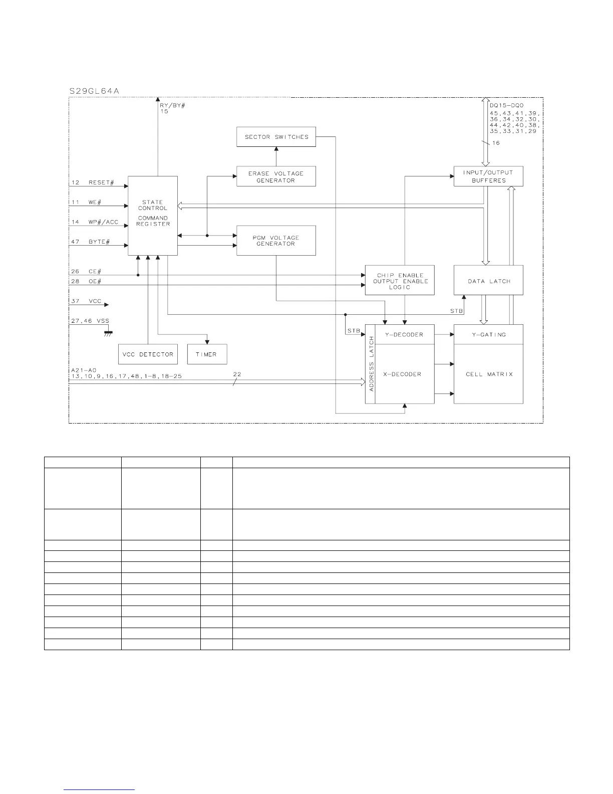
2.13. VHiS29GL64A-1Q (ASSY: IC8451)
64-Mbit Page Mode Flash Memory
• Block Diagram [VHiS29GL64A-1Q (ASSY: IC8451)]
• Pin Function [VHiS29GL64A-1Q (ASSY: IC8451)]
Pin No. Pin Name I/O Pin Function
13, 10, 9, 16, 17,
48, 1, 2, 3, 4, 5, 6,
7, 8, 18, 19, 20, 21,
22, 23, 24, 25
A21-A0 I 22 Address inputs.
43, 41, 39, 36, 34,
32, 30, 44, 42, 40,
38, 35, 33, 31, 29
DQ14-DQ0 I/O 15 Data inputs/outputs.
45 DQ15 I/O DQ15 (Data input/output, word mode).
26 CE# I Chip Enable input.
28 OE# I Output Enable input.
11 WE# I Write Enable input.
14 WP#/ACC I Hardware Write Protect input/Programming Acceleration input.
12 RESET# I Hardware Reset Pin input.
15 RY/BY# O Ready/Busy output.
47 BYTE# I Selects 8-bit or 16-bit mode.
37 Vcc --- 3.0 volt-only single power supply.
27, 46 Vss --- Device Ground.