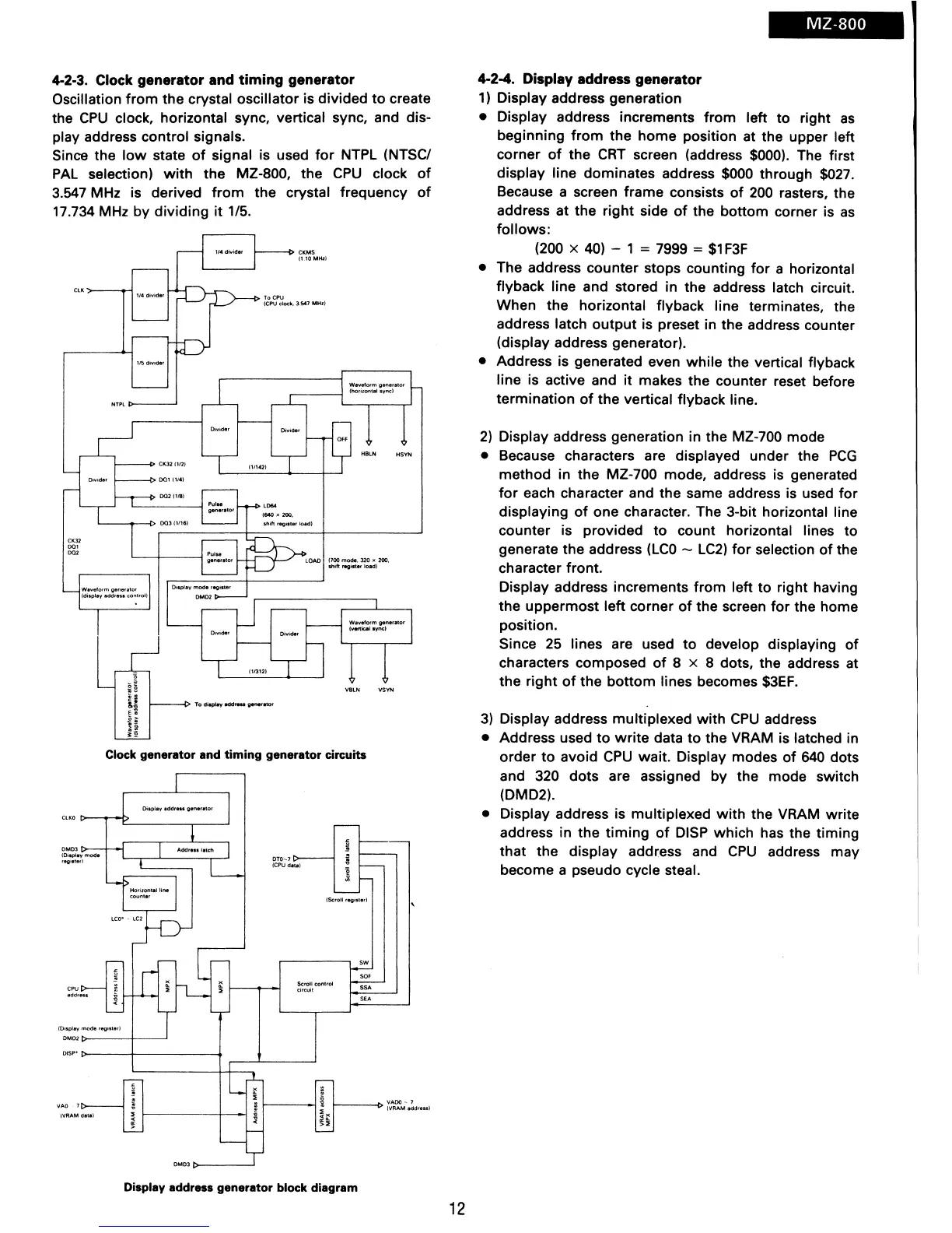
4-2-3. Clock generator and
timing
generator
Oscillation
from
the
crystal oscillator is divided
to
create
the
CPU
clock, horizontal sync, vertical sync, and dis-
play address control signals.
Since the
low
state
of
signal is used
for
NTPL (NTSCI
PAL
selection)
with
the MZ-800, the
CPU
clock
of
3.547 MHz is derived
from
the
crystal frequency
of
17.734 MHz by
dividing
it
1/5.
NTPl
1>-----'
CK32 (112)
001
(114)
To
displ.-v
.dd
.....
generator
Clock generator and
timing
generator
circuits
IO,splay
mode
'egoslll')
OM02
t>----+---'
OTO-7
ICPU
dala)
IScroll regosted
,-----,
sw
Scroll
control
SSA
Display address
generator
block
diagram
VSYN
12
4-2-4. Display address generator
1)
Display address generation
MZ-800
• Display address increments
from
left
to
right
as
beginning
from
the
home
position at the upper left
corner
of
the
CRT
screen (address $000). The first
display line dominates address
$000 through $027.
Because a screen
frame
consists
of
200
rasters, the
address at the
right
side
of
the
bottom
corner is
as
follows:
(200 x 40) - 1 = 7999 =
$1
F3F
• The address counter stops counting
for
a horizontal
flyback line and stored in the address latch circuit.
When the horizontal flyback line terminates, the
address latch
output
is preset in the address counter
(display address generator).
• Address is generated even
while
the vertical flyback
line is active and
it
makes the counter reset before
termination
of
the
vertical flyback line.
2)
Display address generation in the MZ-700 mode
• Because characters are displayed under the
PCG
method
in the MZ-700 mode, address is generated
for
each character and
the
same address is used
for
displaying
of
one character. The 3-bit horizontal line
counter is provided
to
count horizontal lines
to
generate
the
address
(LCO
-
LC2)
for
selection
of
the
character front.
Display address increments
from
left
to
right having
the
uppermost
left corner
of
the screen
for
the home
position.
Since
25
lines are used
to
develop displaying
of
characters composed
of
8 x 8 dots, the address at
the
right
of
the
bottom
lines becomes
$3EF.
3)
Display address
multiplexed
with
CPU
address
• Address used
to
write
data
to
the
VRAM is latched in
order
to
avoid
CPU
wait. Display modes
of
640 dots
and
320
dots
are assigned by the mode switch
(DMD2).
• Display address is
multiplexed
with
the VRAM
write
address in the
timing
of
DISP which has the
timing
that
the display address and
CPU
address may
become a pseudo cycle steal.