27
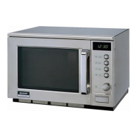
R-22AM
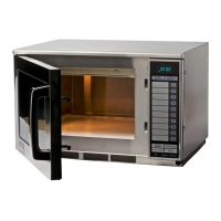
R-23AM
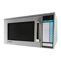
R-23AT
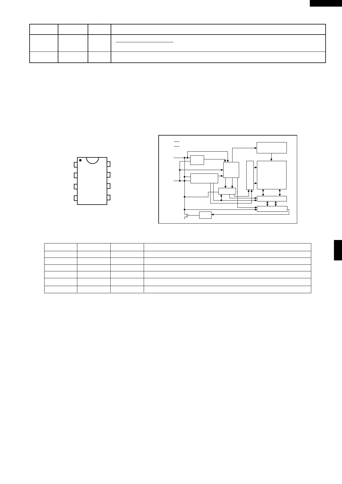
2-2 Memory IC (IC2) FOR R-23AT
AT24C04 is a 4K-bit, serial memory, enabling CMOS to be erased/written electrically. This memory is constructed with
512 registers x 8bits, enabling individual access, read and write operations to be performed. Details of input/output signal
for IC2 are as shown in the following diagram.
Figure T-2. Relation between Pin Nos, and Signals
Pin No. Signal I/O Description
1-3 A0-A2 IN Connected to GND.
4 VSS IN Connected to VC(-5V).
5 SDA IN/OUT Serial data input/output : input/outputs data to IC1.
6 SCL IN Clock signal input : input/outputs serial data at every one pulse.
7 TEST IN Connected to VC(-5V).
8 VCC IN Connected to GND.
Pin No. Signal I/O Description
55-56 P01-P00 OUT Segment data signal.
Signal similar to P21.
57-64 P37-P30 OUT Terminal not used.
A0
81
72
63
54
A1
A2
VSS
VCC
TEST
SCL
SDA
TOP VIEW
FUNCTIONAL DIAGRAM
E PROM
512 x 8
2
START
STOP
LOGIC
CONTROL
LOGIC
SLAVE ADDRESS
REGISTER
COMPARATOR
H.V. GENERATION
TIMING
& CONTROL
64
YDEC
8
DATA REGISTER
Dout
CK
3
1
5
64
XDEC
START CYCLE
INC
LOAD
WORD
ADDRESS
COUNTER
R/W
PIN
Dout
ACK
(6) SCL
(5) SDA
(4) Vss
(3) Vcc