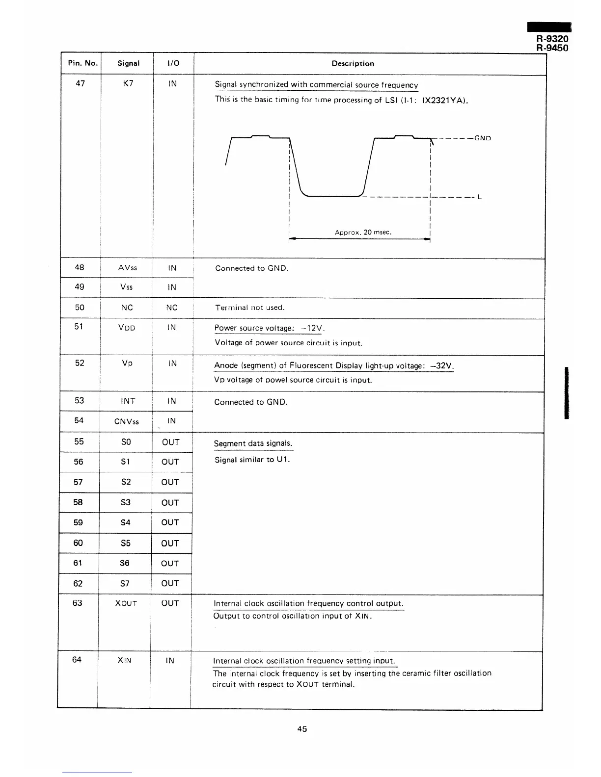
Pin. No. Signal
Description
I/O
IN
47
K7
48
49
AVss
vss
50 NC
Signal synchronized with commercial source frequency
This’ IS the basic timing for time processing of LSI (I-1 : iX2321YA).
~ ~-----_
Approx. 20 msec.
I
1
IN Connected to GND.
IN
NC
Terminal not used.
IN 1
Power source voltage: -12V.
/
I
Voltage of power source circuit is input.
51
VDD
52
VP
IN
Anode (segment) of Fluorescent Display light-up voltage: -32V.
Vp voltage of powel source circuit is input.
53
IN
Connected to GND.
INT
CNVss
54
/
IN /
55
/
OUT /
Segment data signals.
Signal similar to Ul.
so
Sl
56
s2
s3
s4
57
58
59
60
s5 OUT
61
S6
OUT
62
s7
OUT
XOUT OUT
Internal clock oscillation frequency control output.
63
64
Output to control oscillation input of XIN.
XIN IN Internal clock oscillation frequency setting input.
The internal clock frequency is set by inserting the ceramic filter oscillation
circuit with respect to XOUT terminal.
45