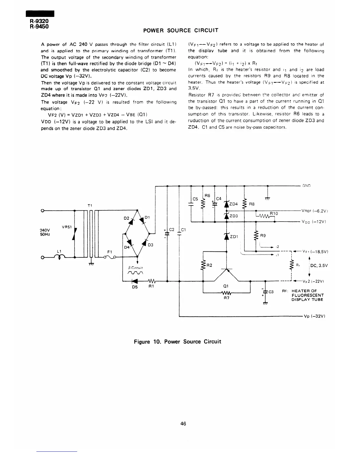
POWER SOURCE CIRCUIT
The voltage VF2 (-22 V) is resulted from the followtng
A power of AC 240 V passes through the filter circuit (Ll)
and is applied to the primary winding of transformer (Tl ).
equation :
The output voltage of the secondary winding of transformer
(Tl) is then full-wave rectified by the diode bridge (Dl - D4)
and smoothed by the electrolytic capacitor (C2) to become
DC voltage Vp (-32V).
vF2 (V) = VZDl + VZD3 + VZD4 - VBE ial)
Then the voltage Vp is delivered to the constant voltage ctrcuit
made up of transistor 01 and zener diodes ZDl, ZD3 and
ZD4 where it is made into VF~ (-22V).
VDD (-12V) is a voltage to be applied to the LSI and it de-
pends on the zener diode ZD3 and ZD4.
(VFl-
VF2) refers to a voltage to be applied to the heater of
the display tube and it is obtained from the followrng
equatron:
(VFl
-vF2) = (il + 12) X Rf
In which, Rf is the heater’s resistor and 11 and i2 are load
currents caused by the resrstors R9 and R8 located In the
heater, Thus the heater’s voltage (VFJ-VF~) IS specified at
3.5v.
the transistor Ql to have a part of the current running In Ql
be by-oassed: this results In a
reduction of the current con-
sumptlon of this transistor.
Ltkewlse, resistor R6 leads to a
ruduction of the current consumption of zener diode ZD3 and
Resistor R7 IS provrded between the collector and emitter of
ZD4. Cl and C5 are noise by-pass capacitors.
VRSl
240V
50Hz
11
D2 d !hDl
it
D4
l-
D5 R’
r T
T
R6
c5
+ c4
ZD4
R8
ZD3
Lmo
T
GIN D
VREF (-6.2V I
I
._ /
T
VDD (--12V)
- !2
I
t
-i1 ,
----~--VW (-18.5V)
R2
8
4
Rc
,
, DC, 3.5V
I
I
I
i
-----I -vF2 (-22v)
Ql
tz c3
Rf: HEATER OF
+
R7
FLUORESCENT
DISPLAY TUBE
m
I
Vp (-32V)
Figure 10. Power Source Circuit
46