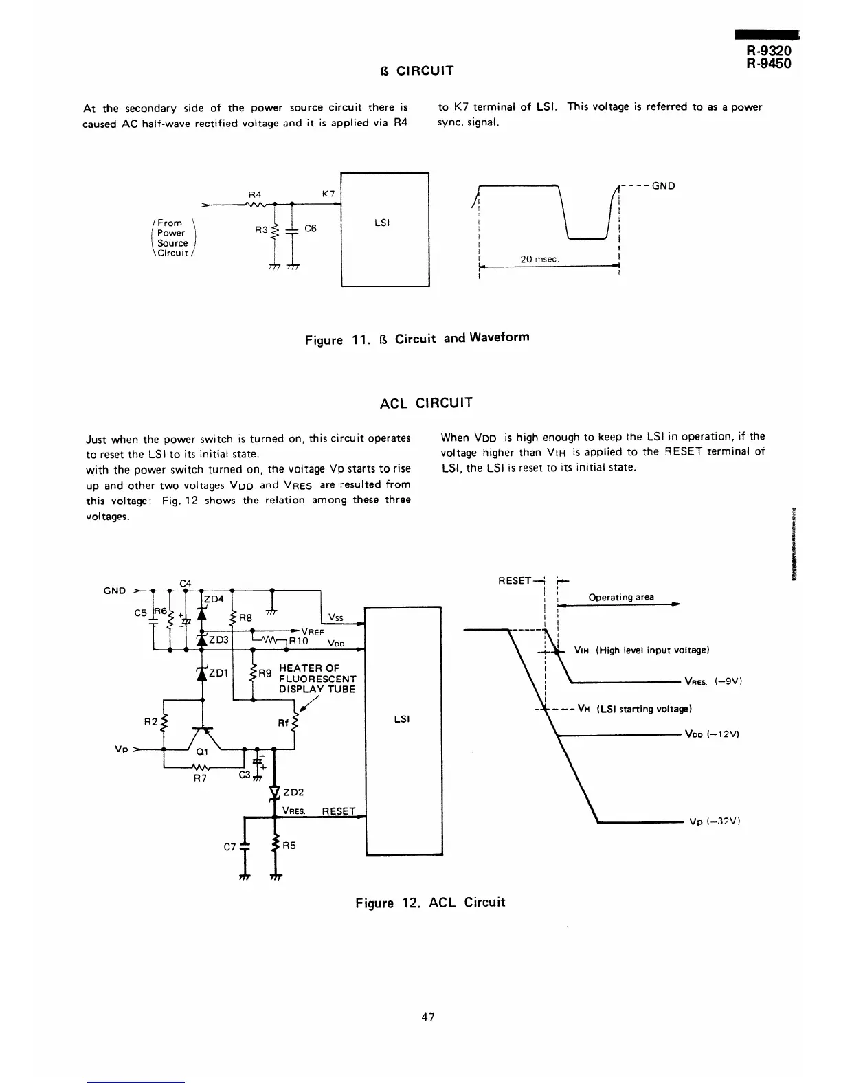
At the secondary side of the power source circuit there is
to K7 terminal of LSI. This voltage is referred to as a power
caused AC half-wave rectified voltage and it is applied via R4
sync. signal.
I3 CIRCUIT
RZ
.
/From
Power
Source
Circuit
R4
K7
\
R3
C6
LSI
i
/
f-1
~--GND
I
20 msec.
I
t=
4
I
I
Figure 11. & Circuit and Waveform
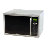
ACL CIRCUIT
Just when the power switch is turned on, this circuit operates
to reset the LSI to its initial state.
with the power switch turned on, the voltage Vp starts to rise
up and other two voltages VDD and VRES are resulted from
this voltage: Fig. 12 shows the relation among these three
voltages.
When VDD is high enough to keep the LSI in operation, if the
voltage higher than VII-I is applied to the RESET terminal of
LSI, the LSI is reset to its initial state.
GND
VP
R9 HEATER OF
FLUORESCENT
DISPLAY TUBE
$
ZD2
c7
LSI
RESETi ”
I ’
Operating area
VIH (High level input voltage)
-
vp (-32VI
Figure 12. ACL Circuit
47