Cycle and Reaction times
3-13
PLC S7-300, CPU Specifications CPU 312 IFM to CPU 318-2 DP
A5E00111190-01
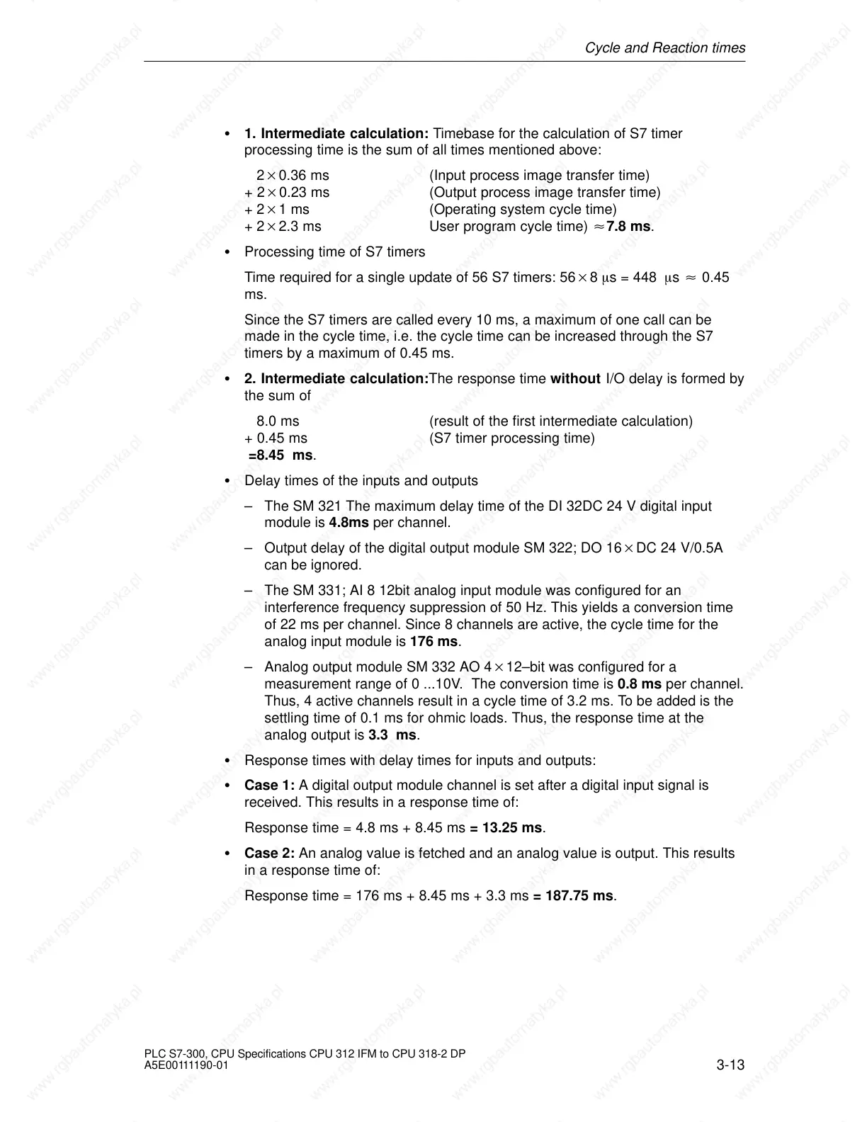
1. Intermediate calculation: Timebase for the calculation of S7 timer
processing time is the sum of all times mentioned above:
20.36 ms (Input process image transfer time)
+ 20.23 ms (Output process image transfer time)
+21 ms (Operating system cycle time)
+22.3 ms User program cycle time) 7.8 ms.
Processing time of S7 timers
Time required for a single update of 56 S7 timers: 568 s = 448 s 0.45
ms.
Since the S7 timers are called every 10 ms, a maximum of one call can be
made in the cycle time, i.e. the cycle time can be increased through the S7
timers by a maximum of 0.45 ms.
2. Intermediate calculation:The response time without I/O delay is formed by
the sum of
8.0 ms (result of the first intermediate calculation)
+ 0.45 ms (S7 timer processing time)
=8.45 ms.
Delay times of the inputs and outputs
– The SM 321 The maximum delay time of the DI 32DC 24 V digital input
module is 4.8ms per channel.
– Output delay of the digital output module SM 322; DO 16DC 24 V/0.5A
can be ignored.
– The SM 331; AI 8 12bit analog input module was configured for an
interference frequency suppression of 50 Hz. This yields a conversion time
of 22 ms per channel. Since 8 channels are active, the cycle time for the
analog input module is 176 ms.
– Analog output module SM 332 AO 412–bit was configured for a
measurement range of 0 ...10V. The conversion time is 0.8 ms per channel.
Thus, 4 active channels result in a cycle time of 3.2 ms. To be added is the
settling time of 0.1 ms for ohmic loads. Thus, the response time at the
analog output is 3.3 ms.
Response times with delay times for inputs and outputs:
Case 1: A digital output module channel is set after a digital input signal is
received. This results in a response time of:
Response time = 4.8 ms + 8.45 ms = 13.25 ms.
Case 2: An analog value is fetched and an analog value is output. This results
in a response time of:
Response time = 176 ms + 8.45 ms + 3.3 ms = 187.75 ms.
 Loading...